Novel computing paradigms on the horizon
Exploring more esoteric approaches to the future of compute
AI is transformational, but increasingly computationally intensive. Future advances will be dependent on discovering new compute methodologies that deliver step-change improvements in both speed and energy efficiency.
Could photonics be the answer?
Photons are virtually frictionless and able to travel much faster than the electrons used in digital microelectronics hence can support higher bandwidths & lower latency whilst also avoiding the resistive losses of electronics to deliver much greater energy efficiency.
This article explores the potential of photonics in the future of AI compute, and the challenges it faces in realising its commercial promise.
Due to the intrinsically linear nature of light, photonics is well suited to supporting the linear algebra used in AI computation.
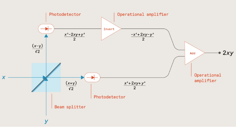
As shown in the following diagram, if two numbers x & y are encoded via the intensity of two light beams sent through a beam splitter, measuring the outputs with photodetectors, and then inverting one before summing, results in a signal proportional to the product of the two numbers (2xy) which can then be stored in a capacitor.

Source: The future of deep learning is photonic [Ryan Hamerly, IEEE Spectrum]; https://spectrum.ieee.org/the-future-of-deep-learning-is-photonic
Subsequent number pairs can be multiplied in the same way, with the products being added together by accumulating charge within the capacitor, the total charge representing the multiply-accumulate (MAC) result.
This process can also be run in parallel by utilising light beams at different wavelengths, with addition being achieved by multiplexing the light beams into a common waveguide, their total optical power representing the MAC result.
MAC computations are a major part of performing the matrix vector multiplication (MVM) used in forward propagation for ML model training and inference. Photonics therefore provides an ideal, energy-efficient way of performing these computations, either via an integrated photonic chip, or conducted in free-space, an approach being explored by Lumai.
Another promising approach pursued by researchers including MIT-based startups Lightmatter and Lightelligence is to use Mach-Zehnder interferometers (MZI) in a 2D array to manipulate light amplitude and phase to perform the matrix multiplication, and by interconnecting the MZIs in a mesh network, compute the product.
Such an approach, utilising both amplitude and phase, extends support to complex numbers thereby enabling support for signal processing in fields such as audio, radar, or communications including, for example, channel estimation where signals are represented as complex data.
In theory then, photonics should be ideal for ML computation. In practise though, scaling it to support large ML models raises a number of challenges.
To begin with, optical computation is analog and inherently imprecise. As the number of waveguides and wavelengths are scaled up, the risk of interference and crosstalk increases, as does the impact of any microscopic imperfections in fabrication with the risk of errors quickly snowballing.
The resulting output is often therefore only an approximation of the matrix multiplication, with reduced bit precision compared to digital systems, and potentially creating a ‘reality gap’ between the trained model and the actual inference output. Manufacturing the photonic chips with higher precision can help to some degree but increases complexity and cost.
Chip size is also an issue. Photonic components tend to be relatively large, limiting chip density. Given that the number of weights (photonic components) squares with the number of neurons, the required chip area for supporting large ML models starts to add up very quickly, increasing cost.
Worst still, if a photonic chip is unable to be scaled large enough to fit the entire ML model, computation requires breaking the model down into chunks and shuttling data between the chip and memory which would necessitate an optical/electrical conversion introducing latency and additional energy consumption.
It’s somewhat ironic that the intrinsic benefit of photonics in increasing the speed and energy efficiency of MVM operations makes most sense at scale, for large ML models, and yet a number of practical limitations preclude achieving this level of scale.
But this isn’t the only challenge – the linearity of light propagation is also both a blessing and a curse.
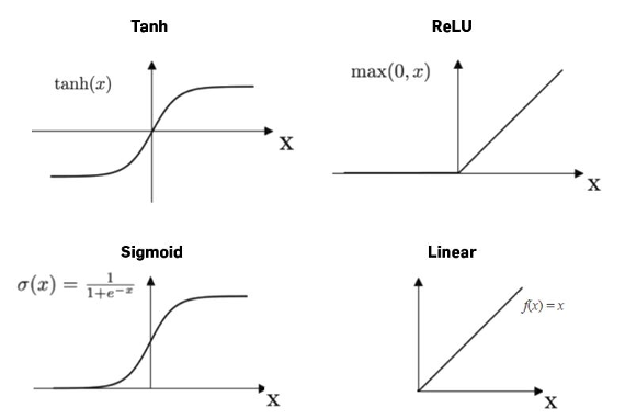
On the one hand, the linearity enables photonics to efficiently compute the weighted sums in MVM operations as we’ve already seen. But in order for ML models to learn complex patterns and represent non-linear relationships, each of these weighted sums also needs to be passed through a non-linear activation function (e.g., ReLU, sigmoid, or softmax), and there’s no easy way of achieving this in photonics.

https://medium.com/@prasanNH/activation-functions-in-neural-networks-b79a2608a106
One approach is to leverage non-linear phenomena such as the Kerr effect or saturable absorption, but these light effects are often weak and require high intensities and/or specialised materials.
Another option is to utilise non-linear modulators, or devices with quantum-dot or phase-change materials (PCM) that exhibit non-linear responses, or perhaps by employing programmable optics or photonic reservoir computing architectures. All though increase complexity and cost.
It’s far easier to simply hand off this computational aspect to digital logic; i.e., perform the linear operations (MVM) using photonics, and send the results to microelectronics for applying the non-linear activation functions.
It’s a similar situation with the process of backpropagation within ML model training which involves computation of gradients – challenging to accomplish solely in photonics, so better handed off to microelectronics.
In practise then, most photonic systems, whether for ML model training or for inference, will most likely need to take a hybrid approach combining both photonics and microelectronics.
But doing so necessitates optical/electrical conversion which introduces latency and energy overhead, as well as noise, and in the case of forward propagation would need to be carried out for each layer within the neural network hence negating much of the speed and energy improvements of conducting the MVM computations photonically in the first place.
Given the maturity of existing AI compute hardware (GPUs, TPUs, and specialised AI accelerators) and their ability to perform billions of MACs per second, photonic alternatives have simply struggled to deliver sufficient performance and cost improvements to justify being considered an attractive “socket-steal”.
For the hybrid photonic approach to become commercially viable it will need to address and improve on the optical/electrical conversion process as well as improve on the speed and energy efficiency of memory access and data movement in general.
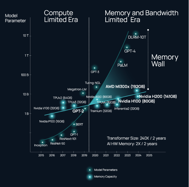
These interconnectivity issues are not limited though to photonic systems, and have become a key limitation in all distributed computing systems and data centre networks, and especially those massively scaled for training and hosting foundational AI models which are starting to hit a ‘memory wall’.

Source: https://www.celestial.ai/technology
The energy consumption associated with shuttling data within and between chips is an escalating problem as demand increases for higher throughput and compute power, and is getting as high as 80% of the total power consumption of a processor; replacing the electronic wires with optical interconnects can improve efficiency by a factor of six.
It’s perhaps not surprising then that many of the photonic startups who originally set out to develop photonic AI accelerators and all-optical computers have turned their attention in the nearer-term to improving the speed and energy efficiency of interconnectivity.
Startups including Lightelligence, Lightmatter, Ayar Labs, Celestial AI, and Black Semiconductor are all developing a range of novel solutions for optical interconnect including graphene-based optoelectronic conversion, optical interposers for connections within and between chiplets within a single chip package, as well as chip-to-chip and node-to-node optical connectivity compatible with standards such as UCIe and CXL, and potentially delivering bandwidth an order of magnitude greater than Nvidia’s NVLink.
That’s not to say that the dream of all-optical compute has been entirely forsaken…
Oxford University, for example, has been exploring ways of combining processing with collocated non-volatile memory based on PCM materials to enable photonic in-memory compute (IMC) and remove the optical/electrical overhead of data movement between the photonic chip and off-chip memory.
Achieving both high speed and low energy consumption has proved challenging, but researchers in the US and Japan have recently devised an efficient non-volatile memory cell using magneto-optical materials that’s compatible with the CMOS fabrication processes used for today’s microelectronics thereby enabling manufacture at scale.
Photonic chip density is another important area for improvement. Neurophos is employing metasurface technology to develop optical modulators 8,000 times smaller than silicon-photonic–based MZIs; more generally, membrane-based nanophotonic technologies should in future enable tens of thousands of photonic components per chip.
Other advancements include the development of very thin nanostructured surfaces that can be combined with semi-transparent mirrors for performing the MVM operations; and in a separate activity scientists have developed an integrated photonics chip capable of nonlinear operations.
Photonics remains a tantalising prospect, with the potential of bringing a much-needed step-change in speed and efficiency to the future of compute for AI.
Many challenges remain though in realising this promise, and doing so with sufficient scale to support large ML models, and even more so given that photonics lags the microelectronics industry in VLSI design tools, yield and manufacturing maturity.
However, with the AI chip market projected to be worth $309bn by 2030 opportunities abound for startups to tackle these challenges and carve a niche with their own innovations.
The US unsurprisingly has a strong cohort of well-funded startups in this space with the likes of Lightmatter, Lightelligence, Ayar Labs and Celestial AI amongst others; but Europe is also strong in photonics AI through startups such as Black Semiconductor and Akhetonics in Germany, and Optalysys, Salience Labs, and Lumai in the UK.
AI is advancing rapidly, and photonics is poised to play a pivotal role in shaping its future, whether that be through all-optical solutions, or nearer-term as a key component in hybrid computing systems.
Exploring more esoteric approaches to the future of compute
Looking beyond NISQ to map out the future timelines for quantum computing