The future of AI compute is photonics… or is it?
Exploring the potential of photonics to improve compute efficiency
Light and its compositions has fascinated scientists for more than 2,000 years – from Aristotle to Newton, Young, Hertz and Maxwell et.al. But it was ultimately Einstein, with his photoelectric effect theory, who postulated that light is made up of particles called photons. Einstein is famous for his research on the theory of relativity yet it was his work on theoretically revealing the photoelectric effect based on the light quantum hypothesis that won him the Nobel Prize in physics in 1921.
The photon has many mysterious physical properties such as possessing the dual properties of a wave and a particle. And it was Einstein himself who described things such as entanglement as “spooky”. Learning more about these properties is allowing us to use light more effectively than ever before and applying this knowledge allows us to make significant advances in many new areas of science and technology. To date, photonics has been predominantly applied to communications with the introduction of optical fibre transforming networks as early as the 1960’s. But now we are seeing photonics taking hold in other areas such as computing, AI, sensing and quantum communications.
In the following brief, David Pollington explores the challenges and exposes some of the early stage innovation opportunities that exist in Photonics and these application areas.
Until now, photonics has focused predominantly on enabling high-speed communications, a lucrative market that now tops $10bn just for optical transceivers. But photonics also has application in many other areas ranging from solid-state LiDAR to inertial navigation sensors, spectrometers, refractive index biosensors, quantum computers, and accelerating AI.
This article discusses the merits of using photons rather than electrons with an especial focus on photonic integrated circuits (PICs), the wide range of integrated photonics use cases, the current industry landscape of PICs, and the opportunities for startups to innovate in this space.
A PIC is a microchip containing photonic components which form a circuit that processes photons as opposed to electrons to perform a function.
In comparison with digital microelectronic circuits in which the majority of functions are performed using transistors, with photonics it’s a little more complex; there’s no single dominant device but rather a variety of components which can be either passive (e.g. couplers, switches, modulators, multiplexers) or active (e.g., amplifiers, detectors, lasers) and then interconnected via waveguides to form a circuit.
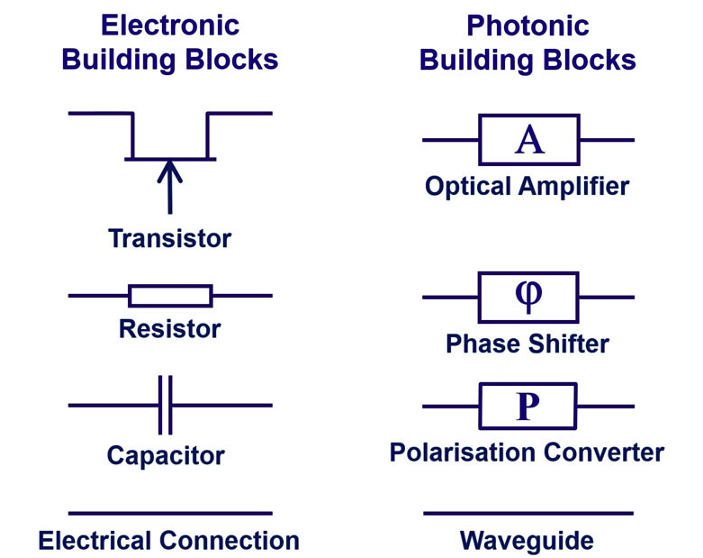
Figure 1: Electronic and photonic circuit building blocks [AIP Publishing]
Similar to digital microelectronics, photonic circuits can be fabricated on silicon, enabling high-density PICs to be made in existing CMOS foundries and co-integrated with transistor-based electronics. Silicon on insulator (SOI) has been the most widely used process within silicon photonics (SiPh) but is likely to be replaced in certain applications by Silicon Nitride (SiN) due to its wider spectral range, low propagation loss and higher power handling (particularly useful for detectors, spectrometers, biosensors, and quantum computers).
However, neither of the silicon-based processes can generate light on their own nor allow for the integration of active components, hence a separate process, Indium Phosphide (InP), is commonly used for fabricating high-performance amplifiers, lasers, and detectors.
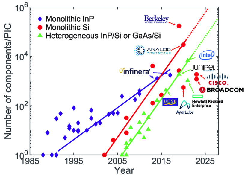
Figure 2: Number of photonic components/PIC [Chao Xiang, University of California]
Photonic circuit design is complex; individual components need to be tailored to the target application requirements (wavelengths; linearities; power levels), process types (SiPh, InP, SiN) and fabs (characterisation), and hence often need to be designed from scratch, requiring large design teams and/or a dependency on independent design houses.
Once the photonic circuit has been designed and verified there are still hurdles in packaging, laser integration, testing and additional processing steps – whilst packaging, assembly, and testing are only a small part of the cost for digital microelectronics (10%), the reverse is true for photonics, and can be as much as 80% of the total cost for InP photonic devices.
Fabs are starting to address this issue by providing process design kits (PDKs) that designers can use to design, simulate, and verify designs before handing them back to the foundry for fabrication. These PDKs include a base set of photonic building blocks (BBs) to bootstrap the design process but are often limited to particular wavelengths and applications (e.g., telecoms).
A market opportunity therefore exists for design houses and other 3rd parties to license out BBs and even entire circuits that fit the broader set of application requirements. LioniX, for example, offers a range of SiN PIC modules, whilst PhotonDelta, a growth accelerator for the Dutch integrated photonics industry, offers a number of design libraries.
EDA tools can then be used for combining these BBs into photonic circuits whilst facilitating seamless integration of electronic and photonic components in IC designs where needed.
However, as mentioned earlier, these designs still then need to be optimised/characterised for the target process/fab, as imperfections and fluctuations of even a few nanometres can cause scattering or reflections and affect performance. In many respects, the photonic circuit design process is more akin to RF and PCB design than digital microelectronics – mostly analogue, and needing careful selection and qualification of components.
A number of parties are exploring ways of addressing some of these issues and accelerating photonic design. Researchers in Canada, for instance, are using machine learning to predict the precise structure of a photonic component once it’s fabricated to a particular process/fab thereby enabling accurate simulation and optimisation to circumvent the ‘trial and error’ nature of photonic design. Similarly, a startup in the UK, Wave Photonics, has pioneered computational techniques to auto-adapt functional building blocks for different wavelengths, fabs and performance design trade-offs.
Nevertheless, the fabrication process still involves a degree of trial and error today, and it may well be 3-5yrs and require a large number of wafer runs and assemblies before the process is perfected sufficiently to deliver the predictable outcomes required to scale up to larger circuits and high volumes.
Digital microelectronics has become pervasive, but with the demand for ever-faster compute and higher-bandwidth networking, the interaction of electrons with other particles in the copper wires at these speeds is resulting in higher energy consumption, more heat, and restrictions to performance. Photons don’t suffer from any of these constraints being virtually frictionless and able to travel faster, support higher bandwidths, and be more energy efficient, hence present an intriguing alternative.
Whilst optical links have been introduced within data centres to form high-speed clusters, the wiring within the racks is typically copper, and as processing demands continue to rise, this is creating a bottleneck and issues around both energy consumption and cooling.
The answer is likely to be through Co-Packaged Optics (CPO) in which the switch ASICs and optical engines are integrated on a single packaged substrate to move the optical connection as close as possible to the switching chip. Doing so enables higher density integration and improves cost effectiveness and energy efficiency with savings of up to 30% of the total system power. Ayar Labs, for example, integrate the optical/electrical components of a transceiver bar the laser inside an optical I/O chiplet.
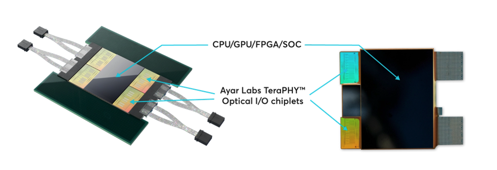
Figure 3: Ayar Labs optical I/O chiplet [Ayar Labs]
In a similar vein, Nvidia and TSMC are interconnecting multiple AI GPUs via a chip-on-wafer-on-substrate (CoWoS) 2.5D package, and Lightmatter’s Passage enables chiplets to be interconnected via nanophotonic waveguides.
The demand for low-power optical transceivers within data centres, and in particular for Co-Packaged Optics (CPO), will be a key driver in the growth of the silicon photonics market over the next 3-5yrs ($3-4 billion by 2025).
With AI compute requirements doubling every 3.4mths (c.f. Moore’s Law which had a 2-year doubling period) [OpenAI] fuelled most recently by the race to generative AI, there is a growing need to develop novel computing systems capable of fast and energy-efficient computation.
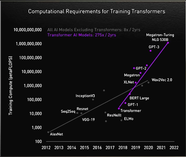
Figure 4: Computational requirements for training transformer models [Nvidia]
Silicon photonics may provide an answer, utilising the unique properties of light to solve complex mathematical problems and meet today’s AI compute demands but with energy consumption as low as one photon per operation and performed at the speed of light hence orders of magnitude faster and more energy efficient than digital computation (although getting data efficiently in/out the photonic chip remains a challenge).
To give an example, detecting edges in an image is of great use in the world of computer vision (e.g., for feature extraction or pattern detection) but requires a lot of compute to perform the CNN multiplication operations.
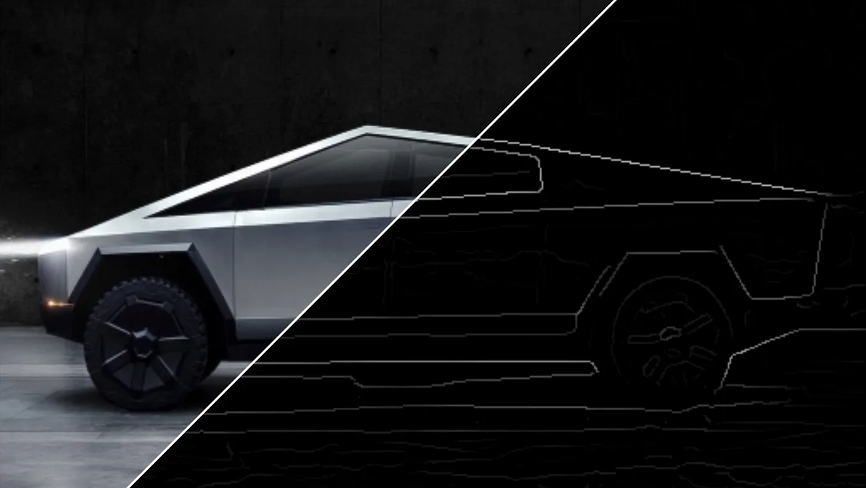
Figure 5: Example of image edge detection [Brighton Nkomo]
Fourier Transforms (FFT) represent a faster method, enabling the image data to be converted from the spatial domain to the frequency domain where edges will be represented by high frequencies which can be captured via a high pass filter. An inverse FFT then transforms the data back into an image showing just the edges of objects in the original image.
The downside is that FFTs themselves are computationally intensive, so this approach presents only a marginal improvement when using digital computation.
Light though has unique properties, and its interference behaviour can be used to perform FFT operations in a massively parallel way that is not only incredibly fast, but also tremendously energy efficient compared to digital computation.
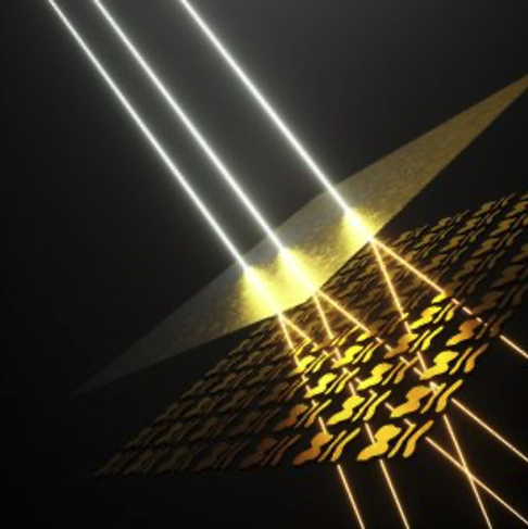
Figure 6: Solving a complex mathematic equation with light [Ella Maru studio]
In practise though, there remain a few obstacles.
Optical components can’t be packed nearly as tightly as transistors hence chip size can be an issue, although membrane-based nanophotonic technologies should in future enable tens of thousands of components per chip, and new approaches such as the use of very thin nanostructured surfaces combined with semi-transparent mirrors are being explored for performing the matrix multiplications in AI/ML inference.
Another issue is around accuracy. Today’s implementations are mainly targeted at performing inference on ML models trained using digital systems. Physical imperfections in the PIC fabrication, and quantisation noise introduced through the optical/electrical converters for getting data in and out of the photonic chip, can result in a ‘reality gap’ between the trained model and inference output that adversely affects accuracy and energy efficiency.
These challenges though present huge opportunity for innovation, whether that be through improving PIC density, optimising the optical/electrical interface to improve precision, or harnessing the unique properties of light to deliver a step-change in AI inference performance and energy efficiency.
Salience Labs for instance are pioneering a novel ‘on-memory compute’ architecture and using different wavelengths of light to facilitate highly parallelised operation and boost performance, whilst Lumai are exploring the application of photonics for more efficient ML model training.
With the AI chip market projected to be worth a colossal $309bn by 2030 [Verified Market Research], the application of integrated photonics to AI acceleration is likely to attract a lot more investor interest and innovation going forward.
At a component level, integrated photonics is being employed in inertial sensors to achieve ultra-precise positioning/indoor navigation [Zero Point Motion], and separately is enabling laser diodes to be integrated with micro-optics and electrical interfaces on a millimetre-sized chip for use in AR/VR glasses as demonstrated in this YouTube video.
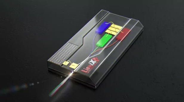
Figure 7: Fully integrated RGB laser light engine for retinal projection in AR [LionIX]
Integrated photonics also opens up the prospect of lab-on-a-chip (LOC) biosensors through a combination of miniaturisation, extreme sensitivity, supporting multiple simultaneous tests, and enabling mass production at low cost. The Point of Care (PoC) market is expected to double in the next few years to $10.1B by 2025 [Yole Development].
Figure 8: Diagnostics platform providing Point of Care (POC) tests [SurfiX Diagnostics]
And finally, the intrinsic benefits in photonics for computing FFTs can also be used to provide the massive vector transforms needed for fast and efficient fully homomorphic encryption (FHE) to enable secure processing in the cloud or by 3rd parties without the data ever being in the clear.
The opportunity is clear. But for integrated photonics to thrive and reach million-scale volumes across multiple sectors there will need to be a more comprehensive set of pre-validated design libraries and tools that decouple design from the underlying fabrication and packaging technology to enable a fabless model that attracts new entrants and innovation.
The opportunity for startups is therefore twofold 1) innovating within the design process & toolchain to reduce lead times and improve performance, 2) applying integrated photonics within new products & services in networking, AI acceleration, ultra-sensitive sensors, and healthcare.
Europe has a heritage in photonics, so it’s perhaps not surprising that European research organisations, spinouts and startups are leading the industry.
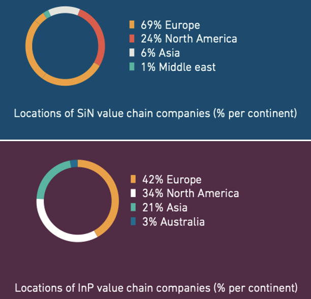
Figure 9: Value chain companies by geography [PhotonDelta: SiN; InP]
In the photonics design, packaging and testing space, example European companies include Alcyon Photonics, Wave Photonics, Bright Photonics, VLC Photonics, Photon Design, FiconTEC, PhotonDelta and LioniX.
Companies developing photonic chips to accelerate AI include Optalysys, Salience Labs and Lumai whilst those using photonics to produce ultra-sensitive sensors include Zero Point Motion, Miraex and PhotonFirst; SMART Photonics and EFFECT Photonics are addressing the telecoms/networking space, and organisations such as PhotonDelta and JePPIX are helping to coordinate the growth of integrated photonics across Europe.
Integrated photonics faces many challenges, but there is increasing evidence that the technology is set to follow the same trajectory as microelectronics over the coming years. The potential upside is therefore huge, both in terms of market value but also in the opportunity this presents for innovative startups.
If you’re a startup in this space, we’d love to hear from you.
Exploring the potential of photonics to improve compute efficiency
Exploring more esoteric approaches to the future of compute