AI is transformational, but increasingly computationally intensive. Future advances will be dependent on discovering new compute methodologies that deliver step-change improvements in both speed and energy efficiency.
Could photonics be the answer?
Photons are virtually frictionless and able to travel much faster than the electrons used in digital microelectronics hence can support higher bandwidths & lower latency whilst also avoiding the resistive losses of electronics to deliver much greater energy efficiency.
This article explores the potential of photonics in the future of AI compute, and the challenges it faces in realising its commercial promise.
Photonics is a natural fit for AI computation
Due to the intrinsically linear nature of light, photonics is well suited to supporting the linear algebra used in AI computation.
As shown in the following diagram, if two numbers x & y are encoded via the intensity of two light beams sent through a beam splitter, measuring the outputs with photodetectors, and then inverting one before summing, results in a signal proportional to the product of the two numbers (2xy) which can then be stored in a capacitor.
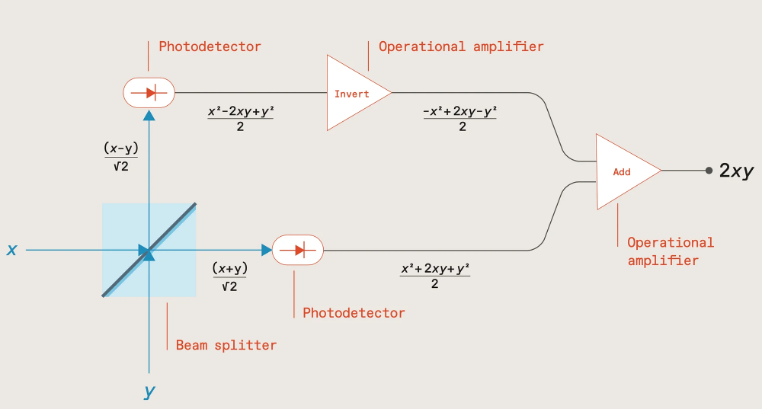
Source: The future of deep learning is photonic [Ryan Hamerly, IEEE Spectrum]; https://spectrum.ieee.org/the-future-of-deep-learning-is-photonic
Subsequent number pairs can be multiplied in the same way, with the products being added together by accumulating charge within the capacitor, the total charge representing the multiply-accumulate (MAC) result.
This process can also be run in parallel by utilising light beams at different wavelengths, with addition being achieved by multiplexing the light beams into a common waveguide, their total optical power representing the MAC result.
MAC computations are a major part of performing the matrix vector multiplication (MVM) used in forward propagation for ML model training and inference. Photonics therefore provides an ideal, energy-efficient way of performing these computations, either via an integrated photonic chip, or conducted in free-space, an approach being explored by Lumai.
Another promising approach pursued by researchers including MIT-based startups Lightmatter and Lightelligence is to use Mach-Zehnder interferometers (MZI) in a 2D array to manipulate light amplitude and phase to perform the matrix multiplication, and by interconnecting the MZIs in a mesh network, compute the product.
Such an approach, utilising both amplitude and phase, extends support to complex numbers thereby enabling support for signal processing in fields such as audio, radar, or communications including, for example, channel estimation where signals are represented as complex data.
In theory then, photonics should be ideal for ML computation. In practise though, scaling it to support large ML models raises a number of challenges.
Scaling photonics is problematic
To begin with, optical computation is analog and inherently imprecise. As the number of waveguides and wavelengths are scaled up, the risk of interference and crosstalk increases, as does the impact of any microscopic imperfections in fabrication with the risk of errors quickly snowballing.
The resulting output is often therefore only an approximation of the matrix multiplication, with reduced bit precision compared to digital systems, and potentially creating a ‘reality gap’ between the trained model and the actual inference output. Manufacturing the photonic chips with higher precision can help to some degree but increases complexity and cost.
Chip size is also an issue. Photonic components tend to be relatively large, limiting chip density. Given that the number of weights (photonic components) squares with the number of neurons, the required chip area for supporting large ML models starts to add up very quickly, increasing cost.
Worst still, if a photonic chip is unable to be scaled large enough to fit the entire ML model, computation requires breaking the model down into chunks and shuttling data between the chip and memory which would necessitate an optical/electrical conversion introducing latency and additional energy consumption.
It’s somewhat ironic that the intrinsic benefit of photonics in increasing the speed and energy efficiency of MVM operations makes most sense at scale, for large ML models, and yet a number of practical limitations preclude achieving this level of scale.
But this isn’t the only challenge – the linearity of light propagation is also both a blessing and a curse.
Solutions needed for non-linear operations
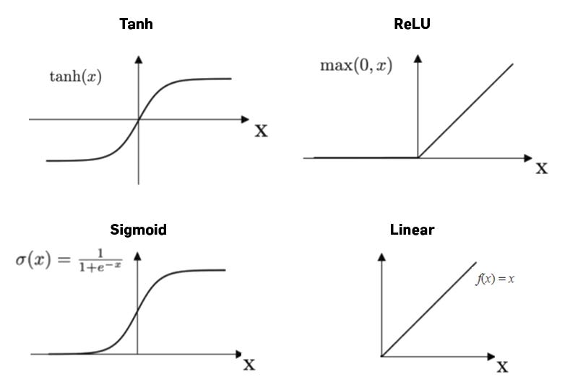
On the one hand, the linearity enables photonics to efficiently compute the weighted sums in MVM operations as we’ve already seen. But in order for ML models to learn complex patterns and represent non-linear relationships, each of these weighted sums also needs to be passed through a non-linear activation function (e.g., ReLU, sigmoid, or softmax), and there’s no easy way of achieving this in photonics.
https://medium.com/@prasanNH/activation-functions-in-neural-networks-b79a2608a106
One approach is to leverage non-linear phenomena such as the Kerr effect or saturable absorption, but these light effects are often weak and require high intensities and/or specialised materials.
Another option is to utilise non-linear modulators, or devices with quantum-dot or phase-change materials (PCM) that exhibit non-linear responses, or perhaps by employing programmable optics or photonic reservoir computing architectures. All though increase complexity and cost.
It’s far easier to simply hand off this computational aspect to digital logic; i.e., perform the linear operations (MVM) using photonics, and send the results to microelectronics for applying the non-linear activation functions.
It’s a similar situation with the process of backpropagation within ML model training which involves computation of gradients – challenging to accomplish solely in photonics, so better handed off to microelectronics.
In practise then, most photonic systems, whether for ML model training or for inference, will most likely need to take a hybrid approach combining both photonics and microelectronics.
But doing so necessitates optical/electrical conversion which introduces latency and energy overhead, as well as noise, and in the case of forward propagation would need to be carried out for each layer within the neural network hence negating much of the speed and energy improvements of conducting the MVM computations photonically in the first place.
Given the maturity of existing AI compute hardware (GPUs, TPUs, and specialised AI accelerators) and their ability to perform billions of MACs per second, photonic alternatives have simply struggled to deliver sufficient performance and cost improvements to justify being considered an attractive “socket-steal”.
For the hybrid photonic approach to become commercially viable it will need to address and improve on the optical/electrical conversion process as well as improve on the speed and energy efficiency of memory access and data movement in general.
These interconnectivity issues are not limited though to photonic systems, and have become a key limitation in all distributed computing systems and data centre networks, and especially those massively scaled for training and hosting foundational AI models which are starting to hit a ‘memory wall’.
Source: https://www.celestial.ai/technology
The energy consumption associated with shuttling data within and between chips is an escalating problem as demand increases for higher throughput and compute power, and is getting as high as 80% of the total power consumption of a processor; replacing the electronic wires with optical interconnects can improve efficiency by a factor of six.
It’s perhaps not surprising then that many of the photonic startups who originally set out to develop photonic AI accelerators and all-optical computers have turned their attention in the nearer-term to improving the speed and energy efficiency of interconnectivity.
Startups including Lightelligence, Lightmatter, Ayar Labs, Celestial AI, and Black Semiconductor are all developing a range of novel solutions for optical interconnect including graphene-based optoelectronic conversion, optical interposers for connections within and between chiplets within a single chip package, as well as chip-to-chip and node-to-node optical connectivity compatible with standards such as UCIe and CXL, and potentially delivering bandwidth an order of magnitude greater than Nvidia’s NVLink.
Fully optical solutions still on the horizon
That’s not to say that the dream of all-optical compute has been entirely forsaken…
Oxford University, for example, has been exploring ways of combining processing with collocated non-volatile memory based on PCM materials to enable photonic in-memory compute (IMC) and remove the optical/electrical overhead of data movement between the photonic chip and off-chip memory.
Achieving both high speed and low energy consumption has proved challenging, but researchers in the US and Japan have recently devised an efficient non-volatile memory cell using magneto-optical materials that’s compatible with the CMOS fabrication processes used for today’s microelectronics thereby enabling manufacture at scale.
Photonic chip density is another important area for improvement. Neurophos is employing metasurface technology to develop optical modulators 8,000 times smaller than silicon-photonic–based MZIs; more generally, membrane-based nanophotonic technologies should in future enable tens of thousands of photonic components per chip.
Other advancements include the development of very thin nanostructured surfaces that can be combined with semi-transparent mirrors for performing the MVM operations; and in a separate activity scientists have developed an integrated photonics chip capable of nonlinear operations.
Takeaways
Photonics remains a tantalising prospect, with the potential of bringing a much-needed step-change in speed and efficiency to the future of compute for AI.
Many challenges remain though in realising this promise, and doing so with sufficient scale to support large ML models, and even more so given that photonics lags the microelectronics industry in VLSI design tools, yield and manufacturing maturity.
However, with the AI chip market projected to be worth $309bn by 2030 opportunities abound for startups to tackle these challenges and carve a niche with their own innovations.
The US unsurprisingly has a strong cohort of well-funded startups in this space with the likes of Lightmatter, Lightelligence, Ayar Labs and Celestial AI amongst others; but Europe is also strong in photonics AI through startups such as Black Semiconductor and Akhetonics in Germany, and Optalysys, Salience Labs, and Lumai in the UK.
AI is advancing rapidly, and photonics is poised to play a pivotal role in shaping its future, whether that be through all-optical solutions, or nearer-term as a key component in hybrid computing systems.
Rapid advances in the digital economy and AI have been driving an ever-increasing need for compute, with an associated impact on energy consumption; keeping pace with this demand long-term is likely to require a fundamental step-change in compute efficiency (performance/Watt).
Previous articles have explored novel computing paradigms including neuromorphic, in-memory compute (IMC), wave-based analog computing and quantum computing. This article identifies some others which could also prove transformative over the coming years.
Reversible computing
In digital logic, when a transistor switches, the previous state is lost, and this process of information deletion transforms into heat according to the laws of thermodynamics and information theory.
Reversible computing, a concept dating back to the 1960s, sets out to remove this intrinsic energy loss through the development of reversible transistors that can revert back to their previous state.
Designing circuits that allow currents to flow both forwards and backwards through the logic gates lessens wear and tear on the transistors thereby increasing chip lifespan as well as reducing power and cooling reqmts.
On the downside, such an approach requires running the chips slower than normal, but the resulting lower performance can be offset by packing chips more densely and stacking in 3D to produce higher performance per unit volume with dramatically lower energy use – in theory, near-zero energy computing.
Implementing this concept in practise is far from trivial, but is now actively being pursued by companies such as Vaire Computing.
Temporal computing
Rather than coding information as 1s and 0s, temporal logic (aka race logic) encodes information as the time it takes for a signal to propagate through the system.
This is similar in some ways to the spiking neural networks (SNNs) discussed within the neuromorphic article, but rather than encoding signals in the number or rate of spikes, temporal computing encodes the time at which the 0 → 1 transition occurs.
Based on four race logic operations, with at most one bit-flip per operation, this enables lower switching activity, higher throughput, and orders-of-magnitude improvement in energy efficiency, albeit sacrificing precision compared to traditional binary representation.
Temporal computing works well for accelerating AI decision-tree classifiers used for categorising images, and is a natural fit for in-sensor processing (image, sound, time-of-flight (ToF) cameras etc.).
It’s less suitable though for generic artificial neural networks (ANNs) due to its inability to perform arithmetic operations like multiplication and addition, although this can potentially be overcome by combining temporal data with pulse rate encoding.
Photonic (optical) computing
In comparison to the electrons used in digital logic, photons are virtually frictionless so able to travel faster (supporting higher bandwidths & lower latency) whilst also consuming much less energy.
This means that matrix multiplication for AI could in theory be performed passively at the ‘speed of light’, and be able to achieve orders of magnitude lower energy consumption by only using one photon per operation.
Source: photonics.com
In practise though, there are a number of challenges faced by photonic computing:
- The optical/electrical converters needed for getting data in and out of the photonic chip constrain throughput and dramatically increase overall power consumption hence diluting the practical energy benefits of photonics
- As an analog calculation, it cannot support floating-point numbers hence is limited to fixed point and low precision (often ≤6 bits)
- Optical components are relatively large and can’t be packed nearly as tightly as transistors, so the required chip area adds up quickly
- Microscopic imperfections in fabrication, and noise introduced through the optical/electrical converters, can result in a ‘reality gap’ between the trained model and inference output that adversely affects accuracy (with errors in the computation quickly snowballing)
- Building a complete photonic computing ecosystem, comprising light sources, passive and active components, and digital logic adds complexity
Photonic computing though still has a lot of promise, and especially so if the optical/electrical conversion process can be sidestepped through the design of an all-optical computer. Akhetonics and others are pursuing such a goal.
For more discussion on photonics and photonic chip (PIC) design, see this previous article.
Reservoir computing
Within the broader field of neuromorphics, reservoir computing (RC) is a relatively new concept that explores ways of developing small, lightweight AI/ML models that are capable of fast inference but also fast adaptation.
Originally conceived in the early 2020s, it follows a similar architecture to ANNs but with a few notable differences. In an ANN, all the parameters are fully trainable whilst in RC the input (sensing) and middle (processing) layers are fixed and it focuses instead on only training the output layer, similar to how many biological neuronal systems work.
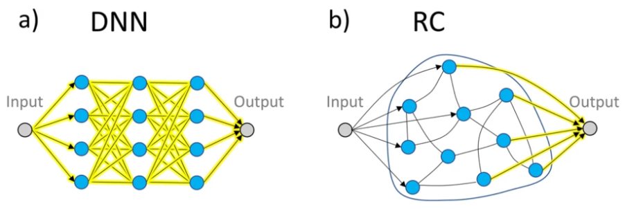
Source: Connecting reservoir computing with statistical forecasting and deep neural networks
The small parameter size and simpler training procedure of reservoir computing leads to reduced training time and resource consumption making it ideal in many industry-level signal processing and learning tasks, such as real-time speech recognition and active noise control amongst others.
It also achieves a surprisingly high level of prediction accuracy in systems that exhibit strong nonlinearity and chaotic behaviour such as in weather forecasting.
Another interesting area being explored is its use within future 6G mobile networks to dynamically model and optimise channel capacity, overturning the traditional passive waveform design and channel coding approach.
Takeaways
For many of the methods discussed in this and previous articles, the concepts actually date back several decades, but due to implementation challenges, and the onward march of conventional digital logic, have remained largely an academic curiosity. With Moore’s Law slowing down, corporates and investors alike are now showing renewed interest in these novel alternatives.
They all show promise in achieving the important step-change needed in compute efficiency (performance/Watt); however, winning widespread commercial adoption will require them to also integrate within established ecosystems.
First and foremost, implementation is still likely to be a challenge, with such capabilities needing to be interfaced with host machines, digital logic, analog/digital conversion and an array of sensors and actuators for use in real-world applications.
In many cases they also take a fundamentally different approach to programming, so achieving adoption will require tools to be provided that can abstract away the underlying idiosyncrasies, and enable these technologies to be easily accessible by existing developer communities, but without diluting any of their unique compute efficiency benefits.
These technologies are unlikely to replace existing xPU compute, at least not in the short-term, but do show real advantages in compute efficiency when applied to specific tasks.
In particular, they’re likely to be indispensable for deploying advanced AI models and computer vision on low-power devices in applications such as autonomous systems (vehicles and drones), robotics, remote sensing, wearable technology, smartphones, embedded systems, and IoT devices.
Interacting with dynamic and often unpredictable real-world environments remains challenging for modern robots, but is exactly the kind of task that biological brains have evolved to solve, and hence is one of the most promising application areas for technologies such as neuromorphics.
For signal processing, a hybrid solution might provide the best of both worlds: analog for approximate computations achieved with high speed using little energy, and digital for programming, storage, and computation with high precision, perhaps using an analog result as a very good initial guess to reduce the problem space. Such hybrid approaches can deliver speedups of 10x whilst also delivering energy savings of a similar magnitude.
And perhaps, with the renewed interest in voice interaction (e.g., ChatGPT’s Advanced Voice Mode; Google’s NotebookLM Audio Overview feature), these technologies could enable voice capabilities to be moved to the edge rather than depend on LLMs in the cloud which may be impractical in situations with poor connectivity, suboptimal in terms of latency, or simply undesirable in the case of sensitive personal or company confidential information.
The future of compute is likely to be heterogeneous, and hence there are a multitude of areas in which startups will be able to innovate and find their niche.
Leveraging the principles of quantum mechanics to establish a new paradigm in computing was first hypothesised four or so decades ago; steady progress has been made since, but it’s really only in the past few years that interest and investment has ramped up, with quantum computing now widely regarded as a cornerstone in the future of compute.
Core to its promise is the introduction of qubits that can represent multiple states simultaneously (superposition) thereby enabling complex problems to be computed in parallel rather than sequentially.
This capability makes it particularly good at solving quadratic optimisation problems in industries such as logistics, finance, and supply chain management. Quantum computers are also intrinsically suited to simulating quantum systems; for instance in drug discovery, where molecular interactions are hard to simulate with classical computers.
Quantum compute power increases exponentially in proportion to the number of qubits available, hence being able to scale the architecture is essential to achieving quantum’s commercial potential.
Simply adding more physical qubits might seem the obvious answer, but results in an escalating error rate due to decoherence, noise, and imperfect operations that limits the current NISQ computers to between 100 to 1,000 reliable quantum operations (QuOps).
Whilst interesting from a scientific perspective, the commercial value of such a capability is limited. To realise its promise, and go beyond the reach of any classical supercomputer (quantum advantage), quantum computing must deliver a million or more QuOps.
Achieving this requires a pivot away from NISQ principles to focus instead on delivering fault-tolerance.
Quantum error correction (QEC) will be key, encoding information redundantly across multiple physical qubits and using sophisticated parity checks to identify and correct for errors; in essence, combining multiple physical qubits to create a logical qubit, an approach validated by research conducted by Google earlier this year and more recently incorporated into their latest quantum chip, Willow.
Provided the physical qubit error rate can be maintained below a critical threshold, every doubling of physical qubits used to generate a logical qubit results in a halving of the overall error rate.
This approach of combining physical qubits to generate logical qubits can then be scaled up to arrange the logical qubits into quantum gates, circuits, and ultimately a quantum computer capable of reaching the targeted million QuOps (a MegaQuOps).
Doing so is likely to require around 50-100 logical qubits, with each logical qubit requiring ~161 physical qubits assuming a 99.9% qubit fidelity – state of the art right now is ~24 logical qubits with Microsoft and Atom Computing looking to commercially launch such a capability next year.
As quantum computers scale further to provide sufficient logical qubits to support trillions of quantum operations, the number of physical qubits per logical qubit also increases (as shown below) and QEC becomes ever more computationally intensive, ironically requiring thousands of classical xPUs to rapidly process the vast amount of syndrome data needed to identify the location and type of each error that needs correcting.
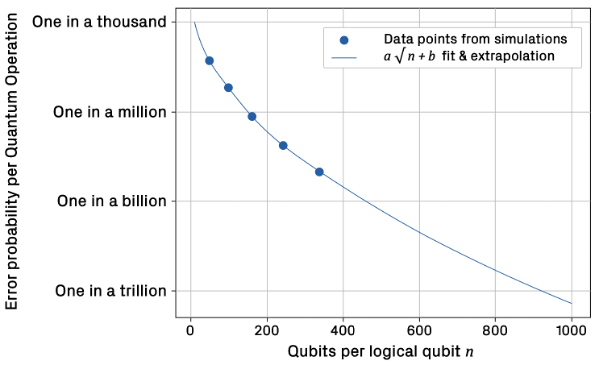
Source: The Quantum Error Correction Report 2024, Riverlane
In short, there’s still a long way to go to reach the million QuOps target, and further still for quantum to deliver on some of the use cases that have driven much of the interest and speculation in quantum computing.
To give an example, it’s estimated that 13 trillion QuOps might be needed to break the RSA encryption used on the Internet (assuming 2048-bit keys), and in doing so realise the so-called quantum threat. This would require error rates to be as low as one in a trillion, far below the one in a thousand achieved in today’s implementations, and might require QEC running at 100TB/s, equivalent to processing Netflix’s total global streaming data every second.
The challenge seems daunting, but steady progress is being made, with the UK Government targeting a million QuOps (MegaQuOp) by 2028, a billion QuOps (GigaQuOp) by 2032 and a trillion (TeraQuOp) by 2035. Others are forecasting similar progress, and see early fault-tolerant quantum computers (FTQC) becoming available within the next five years with MegaQuOp to GigaQuOp capabilities.
In the meantime, rapid advancements in (Gen)AI and massive GPU clusters have enabled AI to encroach on some of the complex problem areas previously thought of as the sole realm of quantum computing – physics, chemistry, materials science, and drug discovery (e.g., Google DeepMind’s AlphaFold, and AlphaProteo) – and caused some to raise doubts about the future role of quantum computing.
In truth though, AI and quantum are not mutually exclusive and are likely to be employed synergistically together as evidenced by Google DeepMind’s AlphaQubit, an AI system that dramatically improves the ability to detect and correct errors in quantum computers.
Longer term, and assuming it can hit its TeraQuOp target, quantum computing may indeed deliver on its promise. And if it can reach ~285 TeraQuOps, quantum may be able to simulate the FeMoCo molecule, improve ammonia production, and in doing so address food scarcity and global warming.
The concept of analog computing dates back to the early 20th century when analog computers were widely used for scientific and industrial applications such as predicting tides and simulating flight dynamics. None other than Claude Shannon, the father of information theory, published on the use of analog computing in solving differential equations back in 1941 for use in physics, engineering, and economics.

Tide-predicting computer; British Association for the Advancement of Science (per Lord Kelvin)
Since then, the definition of analog computing has broadened somewhat, but in basic terms it encompasses one or more of the following:
1. Processing and memory combined in non von Neumann architectures
2. Inherently imprecise & noisy rather than binary and high precision
3. Operates on continuous signals rather than sampling and digitising information
The principle of combining memory elements and processing units has been discussed previously in articles on neuromorphic computing and in-memory compute, the latter also touching on the use of analog techniques to further reduce energy consumption albeit with some notable drawbacks.
This short article explores the third aspect of analog computing, namely the use of continuous signals rather than the discrete binary digits used in modern computing, and in particular wave-based analog computing.
In such an approach, data is encoded in the properties of electromagnetic waves, such as the amplitude, phase, frequency, or polarisation. Mathematical operations can then be carried out by manipulating these wave properties as signals propagate through the system.
By eliminating the inefficiencies of analog/digital conversion, wave computers can operate ‘at the speed of light’, performing operations with extremely low latency and enabling massively parallel computation. Optalysys, for instance, uses this approach to enable more efficient computation of FFTs for fully homomorphic encryption (FHE) in privacy and security applications.
Wave-based analog computers could pave the way for ultra-fast, on-the-fly power-efficient data processing encompassing a range of operations including matrix-vector multiplication, discrete Fourier transforms, filtering, and solving complex matrix equations.
Wave computing can also solve differential equations much faster than their digital counterparts by directly modelling the continuous changes described by the equations. In addition to the fields of physics, engineering and economics mentioned earlier, the techniques can equally be applied in solving equations relevant to biology, fluid dynamics, weather prediction, quantum chemistry, plasma physics, and many other scientific fields.
Ordinarily, such an approach would require bulky optical components, but with the development of metamaterials it has become possible to engineer artificial structures that are carefully designed with respect to their shape, geometry, size, orientation and arrangement to control how electromagnetic waves interact with them thereby enabling subwavelength building blocks and the realisation of chip-level all-optical systems.
Source: https://www.photonics.com/Articles/Optical_Metamaterials_Use_III-V_Semiconductors_as/a61869
On the flip-side, such reliance on metamaterial fabrication limits a given design to specific, fixed functions determined by the physical structure, and precludes the wave computer being easily reconfigured or reprogrammed for different tasks – in this regard, it is more analogous to an ASIC than an xPU.
Another drawback of using metamaterials is their weak non-linearity, hence application has typically been confined to simple linear operations such as image edge detection or matrix multiplications rather than more complex computing tasks requiring strong non-linearities such as in realtime signal processing for use in telecoms and radar systems, or the non-linear activation functions used in ANNs (e.g., ReLU, Sigmoid).
Analog wave-based computing remains an intriguing prospect. Its drawbacks in size and wider applicability has so far limited it to a few specific compute tasks, and hence interest has been more academic than commercial to-date. But in a wider landscape of heterogeneous compute, with different computing paradigms being employed depending on the task, wave-based computing still deserves to be in the mix, and hence an interesting space for startups to explore.
AI has been on a phenomenal rise. Artificial neural network (ANN) accelerators can be extremely performant in executing the multiply accumulate (MAC) operations needed to compute AI. However, keeping them maximally utilised requires rapidly shuttling large amounts of model data between the memory and processing units.
This becomes problematic in von Neumann architectures such as those used in ANN accelerators and modern computing in general where memory and processing are physically separated, and can quickly become a bottleneck that not only affects performance but also results in high energy consumption. In fact, data transfer is becoming more energy-consuming than the ANN computation it supports.
Moving the memory as close to the compute as possible lessens this issue and is the approach often used in ANN accelerators, either by combining memory and compute on the same die, or minimising the distance via 3D hybrid packaging. Such an approach is also popular in vision processors for resource-constrained edge devices, Hailo and Syntiant being good examples.
However, whilst this improves ANN performance, it doesn’t alleviate the bottleneck completely. A better approach, and more in keeping with neuromorphic principles, is to avoid moving the data at all, by conducting the compute operations across a memory array – in-memory compute (IMC).
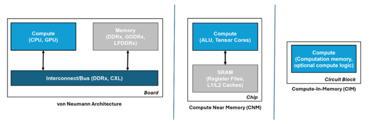
Source: https://gsitechnology.com/compute-in-memory-computational-devices/
Such an approach reduces data transfers to a minimum thereby consuming orders of magnitude less energy than von Neumann architectures, and by minimising the memory bottleneck it also helps to maximise processor utilisation. Moreover, because the IMC elements act inherently as storage, realtime sensor data can be fed into them for immediate ‘through-wire’ processing for realtime edge applications.
Digital IMC
A common approach to IMC is to leverage existing mass production memory technologies such as SRAM and DRAM.
Instead of the usual practise of reading a single bit per memory row, if multiple simultaneous reads are carefully enacted it can provide a NOR function. This opens up the possibility of creating very fast Boolean logic twinned with low energy consumption using just the memory lines.
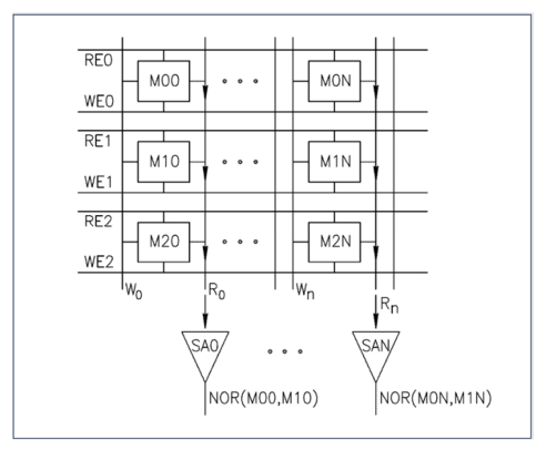
Source: https://gsitechnology.com/compute-in-memory-computational-devices/
Startups such as Synthara and UPMEM are already active in this space developing drop-in replacements for SRAM and DRAM memory chips respectively, and both only requiring minimal software updates to support them. Other startups include d-matrix and MemryX focusing on AI inference acceleration, and RAIN AI, an earlier stage startup yet to bring their solution to market but already targeting a hefty $150m round with support from Sam Altman.
Analog IMC
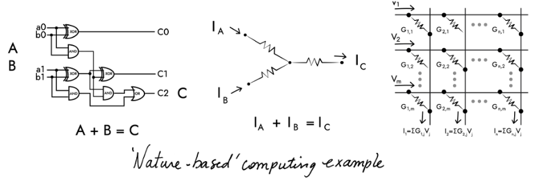
In-memory compute capabilities can also be achieved in the analog domain using a non-volatile memory array, and following a structure more closely aligned with the human brain, with each non-volatile memory element signifying a neuron and interconnections between elements forming a crossbar memory array to emulate the synapses.
Input voltages are applied along the rows of the crossbar array as shown in the diagram below. The output voltage of each neuron is multiplied by its conductance (representing the synapse weight) using Ohm’s Law, and the resulting current is summed up along each column using Kirchhoff’s Law to obtain the dot-product result, equivalent to the MAC operation mentioned earlier.
Source: https://www.aria.org.uk/wp-content/uploads/2023/11/ARIA-Unlocking-AI-compute-hardware-v1.0-1.pdf
Given that the non-volatile memory inherently maintains its state without requiring power, this approach is especially useful for AI inference in those situations where the model weights are seldom updated.
A variety of different implementation technologies are being explored by startups and other companies.
Mythic, for example, are using tuneable resistors (memristors) for the analog memory elements to target low-latency applications such as computer vision, whilst Semron have designed memcapacitive elements to avoid the intrinsic heating of memristive elements and thereby enable die stacking to support large ANNs (e.g., LLMs).
NIST and others have also explored the use of spintronics which exploits the intrinsic spin of electrons, in addition to their charge, to encode and process information. SpinEdge have developed an AI accelerator for edge devices using an array of non-volatile spintronic memory cells for storing the neural network weights.
And finally, IBM have explored the use of multi-level phase-change materials (PCMs) in their Hermes prototype chip. PCMs are particularly good for developing non-volatile memory, and with the added advantage of allowing single bits to be changed without erasing an entire block of cells, hence useful for updating individual model weights.
On the downside, given the analog nature of these different technologies, they suffer from variability across the memory elements which may require retraining of the network after it’s been loaded onto the chip.
Analog can also be limited in terms of precision, and whilst this can be improved by increasing the components’ dynamic range, noise limitations can require higher voltages, and hence higher energy consumption, thus negating the core strength of this approach versus the digital alternatives.
Another consideration is size; by putting all the weights in the crossbars, this can result in a larger chip size compared to the von Neumann approach of fetching the ANN weights as needed. It can also suffer from issues of reliability when scaling to larger systems, and poor area utilisation if the fixed memory array is larger than needed for a given ANN.
Some applications may also require interfacing with digital logic, hence requiring analog/digital conversion which will introduce latency, additional energy consumption, and potentially noise in the ADC/DAC process.
In summary, whilst analog approaches offer advantages in energy efficiency and being able to pre-load ANN models for edge deployment, they also present a number of challenges related to precision, integration, and design complexity that put them, for now, at a disadvantage to their digital equivalents.
Takeaways
As ANN models increase in size, and especially in the case of LLMs with billions of parameters, the energy and performance cost of shuttling data to and from the processing units within the classical von Neumann architecture will become an ever-increasing issue.
Storing the data closer to the processing units is one approach, with the memory elements and processing units ideally being brought together in novel architectures such as in-memory compute.
However, as noted in a previous article on neuromorphic computing, the tight integration of memory and compute might require the memory to be fabricated using the same expensive processes as the digital logic, and this can be 100x the cost of off-chip SRAM or DRAM used in conventional architectures.
And in the case of analog IMC, whilst these approaches show promise in dramatically reducing energy consumption, they also face a number of implementation challenges.
It’s therefore unlikely that in-memory compute solutions will outperform GPUs and ANN accelerators at large scale in data centres.
They are though much better suited to edge applications, such as computer vision, sensing, and robotics where their realtime capabilities are mission critical (Hailo, Syntiant), or in resource-constrained devices such as wearables (Synthara), or more generally for use across a range of edge AI applications in automotive, logistics and IoT (MemryX).
With the race to bring AI applications to the edge this is a vibrant space, and one that’s ripe for startup innovation.
AI has been on a phenomenal rise. But this capability comes at a cost in terms of the compute required for training and inference, and the associated energy consumption. Whilst numerous techniques are being devised for shrinking AI/ML for deployment on edge devices, realising AI’s full potential will require a step-change in compute efficiency (performance/Watt).
The normative approach of packing more transistors into next generation chips (silicon scaling) to boost compute performance has worked well over the past few decades but is starting to become increasingly challenging, and is likely to hit a wall with energy consumption and heat dissipation becoming a limiting factor.
Whilst the energy efficiency of computers has improved by a remarkable 15 orders of magnitude over the past 80 years, the energy required to flip a bit has plateaued and is still 1000x short of the Landauer limit, the theoretical minimum for computation based on information theory. Sending that bit across a chip consumes another 10,000x in energy.
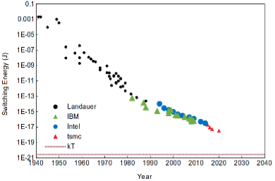
Switching energy per transistor
With physics (silicon scaling) delivering progressively slower gains, researchers are exploring novel architectures that go beyond the limitations of conventional processors to profoundly shift the trajectory for compute efficiency. In particular, researchers have been taking inspiration from the human brain.
The human brain operates 100 billion neurons interconnected by more than 100 trillion synapses to simultaneously compute, reason and store information, and yet consumes a mere 20W. This equates to a power density of 10mW/cm2 compared to a modern processor running an artificial neural network (ANN) that requires 100W/cm2, 4 orders of magnitude more.
At a structural level, ANNs comprise a series of nodes interconnected by weighted links that resemble the neurons and synapses of the brain, but they’re still far from a biological brain in architecture and function.
An important difference is in how the architecture treats storage and compute. The majority of computers follow the von Neumann architecture in which data and compute are logically separated and data is fetched when required for processing.
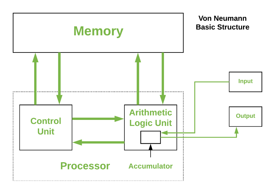
But as noted previously, shuttling data to/from the processor consumes energy and introduces unwanted latency, the so-called von Neumann bottleneck. The brain sidesteps this issue by collocating storage and compute and treating them synonymously.
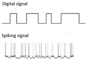
Another major difference is in how information is encoded and processed. Within ANN implementations, input data is encoded as discrete scalars (e.g., pixel values in an image) and clocked through the ANN in a deterministic, synchronous manner to produce an output.
The brain though operates on continuous input values (shaped waves), is stochastic and asynchronous in nature, and effectively encodes information through the timing, magnitude, and shape of spikes that fire between the neurons.
Achieving a similar energy efficiency to the human brain requires a change in both compute architecture and information encoding that more closely mimics the structure and function of the human brain – neuromorphic computing.
Neuromorphic computing
Whilst not a new concept, neuromorphic computing has been receiving a lot of attention lately due to its promise of reducing the computational energy, latency, as well as learning complexity in ANNs. In the last three years alone, there have been over 4.1 million patents filed on neuromorphic computing, with IBM being one of the leaders.
A neuromorphic approach typically incorporates several of the following architecture design principles:
Non von Neumann & distributed (neurons)
Memory and compute are combined in individual, highly distributed processing units analogous to neurons, and highly interconnected similar to the brain’s synapses – mitigates the von Neumann bottleneck.
Inherently parallel
All processing units can be operated simultaneously – massive parallel computation.
Inherently scalable
Blocks of processing units can be combined to create a single large system for running larger and larger ANNs – inherently scalable.
Event-driven
Individual processing units are inherently idle until there is work to be done – event-driven. In conventional ANNs, the neurons and associated processor logic are continuously on, and whilst power gating can be used to switch off parts of the chip, this doesn’t fully exploit the temporally sparse nature of ANNs. With an event-driven approach, the individual processing units are inherently idle until there is work to be done thereby reducing energy consumption by ~2 orders of magnitude compared with typical ANN implementations.
Neuromorphic compute also takes a different approach to information encoding. Today’s ANN implementations are typically state-based and synchronous. The brain is different, conveying information through the use of spikes.
Many neuromorphic implementations therefore employ Spiking Neural Networks (SNNs) that emulate the brain by encoding information similarly through the timing, magnitude, and shape of spikes.
Moreover, they adopt an event-driven methodology whereby the neurons only fire when needed rather than at every propagation cycle as ANN neurons do, and when they do fire, they trigger a huge number of parallel operations via the distributed and highly connected processing units described earlier.
Mechanisms such as spike-timing-dependent plasticity (STDP) adjust the strength of connections between neurons based on the timing of their spikes thereby enabling the SNN to learn from temporal patterns in the data, mimicking the way humans learn from experiences over time.
The key differences between today’s von Neumann compute architecture and the neuromorphic alternative are summarised below:
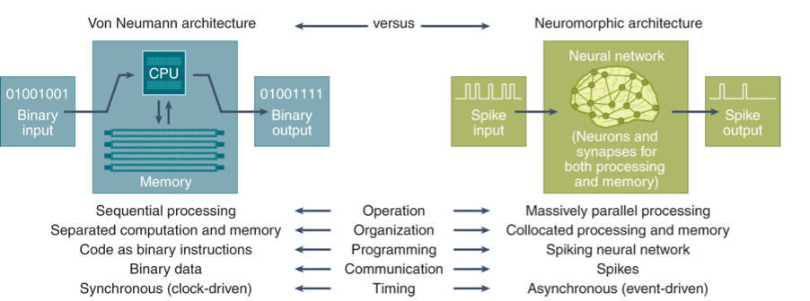
https://www.nature.com/articles/s43588-021-00184-y#Fig1
Neuromorphic implementation options
An easy way to explore and implement a neuromorphic approach is through software. Intel’s open source Lava framework, for example, is designed for asynchronous event-based processing and enables a trained ANN to be converted to an SNN for execution on standard GPUs.
Such an approach offers promising performance and energy reduction by only needing to perform accumulate computations (at the spiking threshold) rather than the multiply and accumulate (MAC) computations intrinsic within an ANN.
Having said that, it doesn’t leverage all the inherent computational capabilities of SNNs (in particular the temporal aspect), and ultimately is limited by the GPU’s von-Neumann architecture it operates on.
Efforts are therefore being made to move instead to purpose-built neuromorphic silicon.
Intel, for instance, have developed the Loihi neuromorphic processor, which in its latest guise (Loihi 2) provides a million computational neurons for complex tasks such as pattern recognition and sensory data processing.
By taking an event-based and asynchronous approach, Loihi’s neurons carry information in both the timing and magnitude of digitally-represented spikes, hence Loihi is extremely energy efficient.
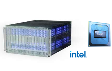
Intel “Hala Point” neuromorphic system
With Hala Point, Intel have created a neuromorphic system comprising over a thousand Loihi 2 neuromorphic processors to achieve a billion neurons – equivalent in size to that of an owl’s brain – and able to solve optimisation problems 50x faster than classical compute and using 100x less energy.
SpiNNcloud, a spinout from the Technical University Dresden, is another player in the neuromorphic space. Leveraging research developed by Dresden within the EU Human Brain Project, they are developing a low-latency and energy-efficient cognitive AI platform combining deep learning, symbolic AI, and neuromorphic computing suitable for a range of AI applications, and with the aim of emulating at least 5 billion neurons.
In a similar vein, Brainchip’s Akida neuromorphic chip combines event-based processing with near-memory compute to target edge applications including advanced driver assistance systems, drones, and IoT devices.
Polyn takes a different route, combining a fixed analog stage that pre-processes sensor input signals with a digital stage providing application-dependent processing to target ultra-low power devices such as wearables.
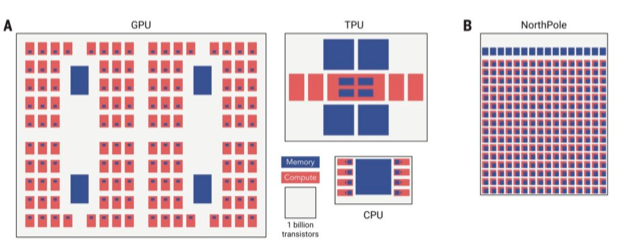
And finally, IBM’s NorthPole chip is an inference-only accelerator comprising 256 computing cores, each of which contains its own memory (memory near compute). By minimising data movement, and utilising lower precision (e.g., INT8, 4 and 2-bit parameters), it has shown high energy efficiency in image classification whilst dispensing with the high-precision typically required for ML training.
Source: https://modha.org
Notwithstanding their differences, these approaches all fit under the neuromorphic banner, and all set out to improve performance and energy efficiency compared to existing solutions.
In practise though, complexities in implementation can negate some of the theoretical benefits. For instance, whilst SNNs involve a simpler accumulation operation than the MAC used in conventional ANNs, the overhead of supporting sparse activation in time- and event-driven computations can result in greater energy usage than today’s highly optimised GPUs and ANN accelerators.
Cost is another important factor. The tight integration of memory and compute in neuromorphic architectures minimises data transfer thereby reducing energy, but on the flip side requires the memory to be fabricated using the same expensive logic processes as the processing units, and this can be 100x the cost of the off-chip DRAM used in conventional architectures.
Given these considerations, neuromorphic is unlikely to outperform GPUs and ANN accelerators at large scale in data centres. It might though be well suited to small-scale, edge-based applications such as voice and gesture recognition, and within mission critical sensing and robotic applications where its low energy and realtime capabilities would be a real benefit.
Other areas being explored include its use within software-defined radio for power-efficient edge devices, and leveraging the massively parallel, event-driven nature of neuromorphic for graph algorithms and optimisation tasks in real-world data modelling.
Neuromorphic is certainly not a panacea for delivering a fundamental step-change in compute efficiency, but in specific targeted applications it shows a lot of promise, and hence represents an interesting area for startups to explore.
Future articles will explore other new compute architectures including in-memory, analog, and of course quantum computing, as well as a few others on the horizon.
Cutting-edge AI/ML models, and especially large language and multimodal models (LLMs; LMMs), are capable of a wide-range of sophisticated tasks, but their sheer size and computational complexity often precludes them from being run locally on devices such as laptops and smartphones.
Usage has therefore been dependent on submitting all queries and data to the cloud, which may be impractical in situations with poor connectivity, suboptimal in terms of latency, or simply undesirable in the case of sensitive personal or company confidential information.
Being able to deploy and run complex AI/ML models on resource-constrained edge devices would unlock opportunities across a swathe of areas including consumer (wearables, smartphones, health monitoring), automotive (computer vision), industrial (predictive maintenance, anomaly detection, AMRs), and space (Earth Observation) amongst others.
Realising these opportunities though is wholly dependent on reducing the computational complexity of the AI/ML models and/or achieving a step-change in compute and energy efficiency at the edge.
Compressing the model to reduce its size is a good first step, and in doing so reduces the memory footprint needed for accommodating the model and the amount of compute and energy needed to run it. Options for reducing model size include quantisation, pruning, and knowledge distillation.
Quantisation
The human brain can simultaneously compute, reason and store information, performing the equivalent of an exaflop whilst using a mere 20W of power. In part, this impressive energy efficiency comes through taking a more relaxed attitude to precision – the same can be applied to ML models.
Quantisation reduces the precision of model weights/activations from the standard 32-bit floating-point numbers (FP32) used when training the model to lower bit widths such as FP8 or INT8 for inference (8-bit integers being much simpler to implement in logic and requiring 10x less energy than FP32).
Doing so risks sacrificing accuracy, but the loss tends to be small (~1%), and can often by recovered through quantisation-aware fine-tuning of the model.
Compression techniques such as GPTQ have enabled AI models to be reduced further down to 3-4 bits per weight, and more recently researchers have managed to reduce model size to as little as 2 bits through the combined use of AQLM and PV-Tuning.
Such an approach though still relies on high precision during training.
An alternate approach is to define low-bitwidth number formats for use directly within AI training and inference. Earlier this year, AMD, Arm, Intel, Meta, Microsoft, NVIDIA, and Qualcomm formed the Microscaling Formats (MX) Alliance to do this with the goal of standardising 6- and 4-bit block floating point formats as drop-in replacements for AI training and inferencing with only a minor impact on accuracy.
Pruning
Another way of reducing model size is to remove redundant or less important weights and neurons, similar to how the brain prunes connections between neurons to emphasise important pathways. Such a technique can typically reduce model size by 20-50% and potentially more, although higher levels require careful fine-tuning after pruning to retain model performance. NVIDIA’s TensorRT, Intel’s OpenVINO, Google LiteRT and PyTorch Mobile all offer a range of tools for model pruning, quantisation and deployment to edge devices.
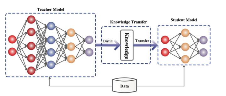
Knowledge distillation & SLMs
In situations where the required functionality can be clearly defined, such as in computer vision or realtime voice interfaces, it may be possible to employ a much smaller language model (SLM) that has been specifically trained for the task.
Such models can be developed either through a process of knowledge distillation, in which a smaller network is taught step by step using a bigger pre-rained network, or through training using a highly curated ‘textbook quality’ dataset.
Source: https://arxiv.org/abs/2006.05525
Microsoft’s Phi-3, for example, is a 3.8B parameter model that is 50x smaller than the flagship LLMs from OpenAI et al but with similar performance in the specific capabilities targeted. The forthcoming Copilot+ laptops will include a number of these SLMs, each capable of performing different functions to aid the user.
Apple have similarly adopted the SLM approach for the iPhone, but differ by combining a single pre-trained model with curated sets of LoRA weights that are loaded into the model on demand to adapt it to different tasks rather than needing separate models. By further shrinking the model using 3.5bits per parameter via quantisation, they’ve managed to squeeze the performance of an LLM into the recently launched iPhone 16 (A18 chip: 8GB, 16-core Neural Engine, 5-core GPU) to support their Apple Intelligenceproposition.
This is a vibrant and fast moving space, with research teams in the large AI players and academia continually exploring and redefining the art of the possible. As such, it’s a challenging environment for startups to enter with their own algorithmic innovations and successfully compete, although companies such as TitanML have developed a comprehensive inference stack employing Activation-aware Weight Quantization (AWQ), and Multiverse Computing have successfully demonstrated the use of Quantum-inspired tensor networks for accelerating AI and cutting compute costs.
Opportunities also exist in situations where a startup has privileged access to a sector-specific dataset and hence is able to generate fine-tuned AI solutions for addressing particular industry pain points at the edge – few have surfaced to-date, hence this remains a largely untapped opportunity for startups to explore with suitable strategic partners.
To fully democratise the use of AI/ML, and LLMs/LMMs in particular, will though also require a step change in compute performance and energy efficiency at the edge. Later articles will dive into the future of compute, and explore novel architectures including neuromorphic, in-memory, analog, and of course quantum computing, as well as a few others on the horizon.
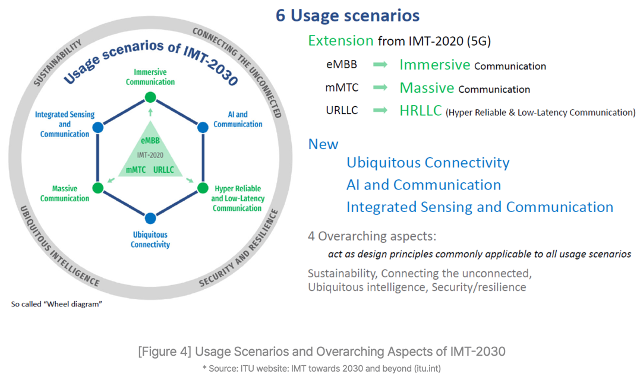
The mobile industry has been marching to the constant drum beat of defining, standardising and launching the next iteration of mobile technology every ten years or so – 3G launching in 2001, 4G in 2009, 5G in 2019, and now 6G mooted for 2030 if not before.
The ITU have laid out a set of 6G goals for the industry to work towards in the IMT-2030 framework. It builds on the existing 5G capabilities, with the aim of 6G delivering immerse, massive, hyper-reliable and low latency communications as well as increasing reach and facilitating connected intelligence & AI services.
In the past, each successive iteration has demanded wholesale upgrades of the network infrastructure – great for the telco equipment manufacturers, but ruinous for the mobile network operators (MNOs).
The GSMA and McKinsey estimate that MNOs worldwide have invested somewhere between $480 billion and $1 trillion respectively to fund the rollout of 5G. And whilst 5G has delivered faster network speeds, there are precious few examples of where 5G has delivered incremental value for the MNOs.
MNOs remain unconvinced that there are any new apps on the horizon that need ‘a new G’, and hence the likes of AT&T, Orangeand SKT amongst others have been vocal about an evolution of 5G rather than yet another step-change with 6G.
This sentiment has been further reinforced by the wider MNO community through NGMN with a clearly stated position that 6G should entail software-based feature upgrades rather than “inherently triggering a hardware refresh”.
The NGMN 6G Position Statement goes on to set a number of MNO-endorsed priorities focused primarily on network simplification with the goal of lowering operational costs, rather than the introduction of whizzy new features.
In particular, it emphasises “automating network operations and orchestration to enable efficient, dynamic service provisioning”, and “proactive network management to predict and address issues before they impact user experience”.
AI will play a pivotal role in achieving these aims. Machine learning (ML) models, for instance, could be trained on a digital twin of the physical environment and then transferred to the network to optimise it for each deployment site, radio condition, and device/user context, thereby improving performance, quality of service (QoS), and network robustness.
AI could also be used to address power consumption, another concern for MNOs, with energy costs representing as much as 40% of a network‘s OPEX according to the GSMA, and now outpacing MNO sales growth by over 50%.
By analysing traffic patterns and other factors, AI is able to make predictions on future traffic demand and thereby identify where parts of the network could be temporarily shut down, reducing energy consumption by 25% and with no adverse impact on the perceived network performance. Turkcell, for example, found that AI was able to reduce their energy consumption by ~63GWh, equivalent to the energy required by OpenAI to train GPT-4.
Startups such as Net.AI have been pioneering in this space, applying AI to improve the energy efficiency of network infrastructure, whilst EkkoSense have recently helped VM O2 save over £1 million a year in the cost of cooling its data centres, and Three have been working with Ericsson to improve energy efficiency by ~70% through the use of AI, data analytics and a ‘Micro Sleep’ feature.
Progressive MNOs such as SKT and Verizon have set out clear strategies for embracing AI, with SKT also teaming up with DT, e&, and Singtel to develop large language models for automating aspects of customer services (Telco LLM) as part of the Global Telco AI Alliance.
Given its staid image, it may be surprising to learn that telecoms is leading the adoption of GenAI (70%) ahead of both the retail (66%) and banking & insurance (60%) sectors. 89% of telcos plan to invest in GenAI next financial year – the joint highest along with the insurance industry – with application across marketing, sales and IT.
Wider adoption though of AI across all aspects of mobile won’t be easy, and certainly the integration of AI natively into future mobile networks to achieve the desired performance and energy efficiency benefits will present a few challenges.
Naysayers argue that there will be insufficient data to model all network eventualities, and that energy optimisation will be hampered given that much of the passive infrastructure at basestations (power management; air conditioning etc.) is not IP-connected.
Interoperability is another concern, particularly in the early days where AI systems are likely to be developed and deployed independently, hence creating a risk of inadvertently working against each other (e.g., maximising network performance vs shutting down parts of the network to conserve energy).
Other MNOs including Orange baulk at the cost of acquiring sufficient compute to support AI given the current purchasing frenzy around GPUs, and the associated energy cost.
This is likely to be mitigated in the longer term through combining telco and AI compute in an AI-native virtualised network infrastructure. Ericsson, T-Mobile, Softbank, NVIDIA, AWS, ARM, Microsoft, and Samsung have recently joined forces to form the AI-RAN Alliance with the goal of developing AI-integrated RAN solutions, running AI and virtualised network functions on the same compute to boost network efficiency and performance.
NVIDIA and Softbank have already run a successful pilot, demonstrating carrier-grade 5G performance on an Nvidia-accelerated AI-RAN solution whilst using the network’s excess capacity to run AI interference workloads concurrently. In doing so, they were able to unlock the two thirds of network capacity typically running idle outside of peak hours for additional monetisation, effectively turning network base stations from cost centres into AI revenue-producing assets – Nvidia and SoftBank estimate that an MNO could earn ~$5 in AI inference revenue for every $1 capex invested in new AI-RAN infrastructure.
As mentioned earlier, many MNOs are already experimenting with AI across different aspects of their network and operations. To-date, this has typically involved employing in-house resources in limited pilots.
Going forward, it’s likely that AI will only realise its true potential through fostering a closer collaboration between the telecoms and AI sectors (cf. GSMA/ATI 2019), and opening up the network to embrace 3rd party innovation for tackling operational efficiency, a market potentially worth $20 billion by 2030.
This is a contentious issue though; whilst MNOs have been moving gradually towards a more open network architecture through adoption of network function virtualisation and participation in industry initiatives such as O-RAN that target network disaggregation, at an operational level many MNOs still prefer procuring from incumbent suppliers and resist any pressure to diversify their supply chain.
Taking such a stance presents a number of hurdles for startups hoping to innovate in network AI, and worst still, the lack of a validated channel-to-market disincentivises any funding of said startups by VCs.
Elsewhere, there may be other opportunities; for instance, in private 5G where solutions can be curated and optimised for individual Enterprise customers, or in the deployment of neutral host networks at public hotspots run by local councils or at stadiums – a £40m UK Gov initiative is currently underway to fund pilots in these areas.
There may also be opportunities to innovate on top of public 5G, leveraging new capabilities such as network slicing to deliver targeted solutions to particular verticals such as broadcasting and gaming, although this hinges on MNO rollout of 5G Standalone, which has been a long time coming, and making these capabilities available to developers via APIs.
MNOs have tried exposing network capabilities commercially many times in the past, either individually or through industry initiatives such as One API Exchange and the Operator Platform Group, but with little success.
MobiledgeX, an edge computing platform spanning 25 MNOs across Europe, APAC and North America was arguably more successful, but eventually acquired and subsumed into Google Cloud in 2022.
Since then, MNOs have progressively come to terms with the need to partner with the Hyperscalers, and more recently Vodafoneand BT amongst others have signed major deals with the likes of Google, Microsoft and AWS.
More interestingly, a collection of leading MNOs (Vodafone; AT&T; Verizon; Bharti Airtel; DT; Orange; Telefonica; Singtel; Reliance Jio; Telstra; T-Mobile US; and America Movil) have recently teamed up with Ericsson and Google Cloud to form a joint venture for exposing industry-wide CAMARA APIs to foster innovation over mobile networks.
If they get it right this time, they may succeed in attracting startups and developers to the telecoms sector, and in doing so unlock a potential $300bn in monetising the network as a platform, as well as expanding their share of the worldwide $5 trillion ICT spend.
The New Space era
The space industry has seen rapid change over the past decade with increased involvement from the private sector dramatically reducing costs through innovation, and democratising access for new commercial customers and market entrants – the New Space era.
Telecoms in particular has seen recent growth with the likes of Starlink, Kuiper, Globalstar, Iridium and others all vying to offer a mix of telecoms, messaging and internet services either to dedicated IoT devices and consumer equipment in the home or direct to mobile phones through 5G non-terrestrial networks (NTN).
Earth Observation (EO) is also going through a period of transformation. Whilst applications such as weather forecasting, precision farming and environmental monitoring have traditionally involved data being sent back to Earth for processing, the latest EO satellites and hyperspectral sensors gather far more data than can be quickly downlinked and hence there is a movement towards processing the data in orbit, and only relaying the most important and valuable insights back to Earth; for instance, using AI to spot ships and downlink their locations, sizes and headings rather than transferring enormous logs of ocean data.
Both applications are dependent on higher levels of compute to move signal processing up into the satellites, and rapid development and launch cycles to gain competitive advantage whilst delivering on a constrained budget shaped by commercial opportunity rather than government funding.
Space is harsh
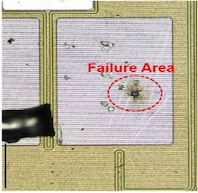
The space environment though is harsh, with exposure to ionising radiation degrading satellite electronics over time, and high-energy particles from Galactic Cosmic Rays (GCR) and solar flares striking the satellite causing single event effects (SEE) that can ‘upset’ circuits and potentially lead to catastrophic failure.
The cumulative damage is known as the total ionising dose (TID) and has the effect of gradually shifting semiconductor gate biasing over time to a point where the transistors remain permanently open (or closed) leading to component failure.
In addition, the high-energy particles cause ‘soft errors’ such as a glitch in output or a bit flip in memory which corrupts data, potentially causing a crash that requires a system reboot; worst case, they can cause a destructive latch-up and burnout due to overcurrent.
Radiation-hardening
The preferred method for reducing these risks is to use components that have been radiation-hardened (‘rad-hard’).
Historically this involved using exotic process technologies such as silicon carbide or gallium nitride to provide high levels of immunity, but such an approach results in slower development time and significantly higher cost that can’t be justified beyond mission-critical and deep-space missions.
Radiation-Hardening By Design (RHBD) is now more common for developing space-grade components and involves a number of steps, such as changes in the substrate for chip fabrication to lower manufacturing costs, switching from ceramic to plastic packaging to reduce size and cost, and specific design & layout changes to improve tolerance to radiation. One such design change is the adoption of triple modular redundancy (TMR) in which mission critical data is stored and processed in three separate locations on the chip, with the output only being used if two or more responses agree.
These measures in combination can provide protection against radiation dose levels (TID) in the 100-300 krad range – not as high as for fully rad-hard mission-critical components (1000 krad+), but more than sufficient for enabling multi-year operation with manageable risk, and at lower cost.
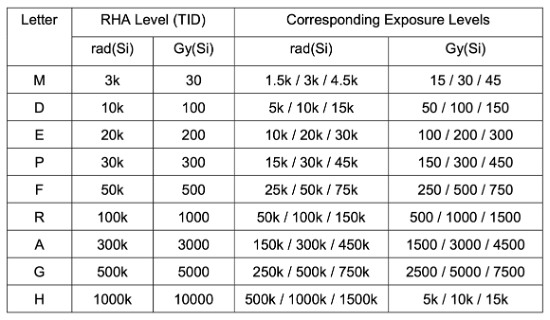
ESCC radiation hardness assurance (RHA) qualification levels
Having said that, they still cost much more than their commercial-off-the-shelf (COTS) equivalents due to larger die sizes, numerous design & test cycles, and smaller manufacturing volumes. RHBD components also tend to shy away from employing the latest semiconductor technology (smaller CMOS feature sizes, higher clock rates etc.) in order to maximise radiation tolerance, but in doing so sacrifice compute performance and power efficiency.
For today’s booming space industry, it will be challenging for space-grade components alone to keep pace with the required speed of innovation, high levels of compute, and constrained budgets driven by many New Space applications.
The challenge therefore is to design systems using COTS components that are sufficiently radiation-tolerant for the intended satellite lifespan, yet still able to meet the performance and cost goals. But this is far from easy, and the march to ever smaller process nodes (e.g., <7nm) to increase compute performance and lower power consumption are making COTS components increasingly vulnerable to the effects of radiation.
Radiation-tolerance
Over the past decade, the New Space industry has experimented with numerous approaches, but in essence the path most commonly taken to achieve the desired level of radiation tolerance for small satellites is through a combination of upscreening COTS components, dedicated shielding, and novel system design.
Upscreening
The radiation-tolerance of COTS components varies based on their internal design & process node, intended usage, and variations and imperfections in the chip-manufacturing process.
Typically withstanding radiation dose levels (TID) in the 5-10 krad range before malfunction, some components, such as those designed for automotive or medical applications and manufactured using larger process nodes (e.g., >28nm), may be tolerant up to 30-50 krad or even higher whilst also being better able at coping with the vibration, shock and temperature variations of space.
A process of upscreening can therefore be used to select components with better intrinsic radiation tolerance, and then filter out those with the highest tolerances within a batch.
Whilst this addresses the degradation over time due to ionising radiation, the components will still be vulnerable to single event effects (SEE) caused by high-energy particles, and even more so if they are based on smaller process nodes and pack billions of transistors into each chip.
Shielding
Shielding would seem the obvious answer, and can reduce the radiation dose levels whilst protecting to some extent against the particles that cause SEE soft errors.
Typically achieved using aluminium, shield performance can be improved by increasing its thickness and/or coating with a high-density metal such as tantalum. However, whilst aluminium shielding is generally effective, it’s less useful with some high-energy particles that can scatter on impact and shower the component with more radiation.
The industry has more recently been experimenting with novel materials, one example being the 3D-printed nanocomposite metal material pioneered by Cosmic Shielding Corporation that is capable of reducing the radiation dose rate by 60-70% whilst also being more effective at limiting SEE.
Concept image of a custom plasteel shielding solution for a space-based computer (CSC)
System design
Careful component selection and shielding can go a long way towards achieving radiation tolerance, but equally important is to design in a number of fault management mechanisms within the overall system to cope with the different types of soft error.
Redundancy
Similar to TMR, triple redundancy can be employed at the system level to spot and correct processing errors, and shut down a faulty board where needed. SpaceX follows such an approach, using triple-redundancy within its Merlin engine computers, with each constantly checking on the others as part of a fault-tolerant design.
System reset
More widely within the system, background analysis and watchdog timers can be used to spot when a part of the system has hung or is acting erroneously and reboot accordingly to (hopefully) clear the error.
Error correction
To mitigate the risk of data becoming corrupted in memory due to a single event upset (SEU), “scrubber” circuits utilising error-detection and correction codes (EDAC) can be used to continuously sweep the memory, checking for errors and writing back any corrections.
Latch-up protection
Latch-ups are a particular issue and can result in a component malfunctioning or even being permanently damaged due to overcurrent, but again can be mitigated to some extent through the inclusion of latch-up protection circuitry within the system to monitor and reset the power when a latch-up is detected.
This is a vibrant area for innovation within the New Space industry with a number of companies developing novel solutions including Zero Error Systems, Ramon Space, Resilient Computing and AAC Clyde Space amongst others.
Design trade-offs
Whilst the New Space industry has shown that it’s possible to leverage cheaper and higher performing COTS components when they’re employed in conjunction with various fault-mitigation measures, the effectiveness of this approach will ultimately be dependent on the satellite’s orbit, the associated levels of radiation it will be exposed to, and its target lifespan.
For the New Space applications mentioned earlier, a low earth orbit (LEO) is commonly needed to improve image resolution (EO), and optimise transmission latency and link budget (telecoms).
Orbiting at this altitude though results in a shorter satellite lifespan:
- More residual atmosphere and microscopic debris slow the satellite down and require it to burn more propellant to maintain orbit
- Debris also gradually degrades the performance of the solar panels
- More time is spent in the Earth’s shadow, thereby causing batteries to go through multiple discharge/recharge cycles per day which reduces their lifetime
Because of this degradation, LEO satellites may experience a useful lifespan limited to ~5-7yrs (Starlink 5yrs; Kuiper 7yrs), whilst smaller CubeSats typically used for research purposes may only last a matter of months.
Given these short periods in service, the cumulative radiation exposure for LEO satellites will be relatively low (<30 krad), making it possible to design them with upscreened COTS components combined with fault management and some degree of shielding without too much risk of failure (and in the case of telecoms, the satellite constellations are complemented with spares should any fail).
With CubeSats, where lifetime and hence radiation exposure is lower still (<10 krad), and the emphasis is often on minimising size and weight to reduce costs in manufacture and launch, dedicated shielding may not be used at all, with reliance being placed instead on radiation-tolerant design at the system level… although by taking such risks, CubeSats tend to be prone to more SEE-related errors and repeated reboots (possibly as much as every 3-6 weeks).
Spotlight on telecoms
In the telecoms industry, there is growing interest in deploying services that support direct-to-device (D2D) 5G connectivity between satellites and mobile phones to provide rural coverage and emergency support, similar to Apple’s Emergency SOS service delivered via Globalstar‘s satellite constellation.
To-date, constellations such as Globalstar’s have relied on simple bent-pipe (‘transparent’) transponders to relay signals between basestations on the ground and mobile devices. Going forward, there is growing interest in moving the basestations up into the satellites themselves to deliver higher bandwidth connectivity (a ‘regenerative’ approach). Lockheed Martin, in conjunction with Accelercomm, Radisys and Keysight, have already demonstrated technical feasibility of a 5G system and plan a live trial in orbit later in 2024.

Source: Lockheed Martin
The next few years will see further deployments of 5G non-terrestrial networks (NTN) for IoT and consumer applications as suitable space-grade and space-tolerant processors for running gNodeB basestation software and the associated inter-satellite link (ISL) processing become more widely available, and the 3GPP R19 standards for the NTN regenerative payload approach are finalised.
Takeaways
New Space is driving a need for high levels of compute performance and rapid development using the latest technology, but is limited by strict budgetary constraints to achieve commercial viability. The space environment though is harsh, and delivering on these goals is challenging.
Radiation-hardening of electronic components is the gold standard, but expensive due to the lengthier design & testing cycles, and higher marginal cost of manufacturing due to the smaller volumes, and such an approach often needs to sacrifice compute performance to achieve higher levels of radiation immunity and longer lifespan.
COTS components can unlock higher levels of compute performance and rapid development, but are typically too vulnerable to radiation exposure to be used in space applications on their own for any appreciable length of time without risk of failure.
Radiation-tolerance can be improved through a process of upscreening components, dedicated shielding, and fault management measures within the system design. And this approach is typically sufficient for those New Space applications targeting LEO orbits which, due to the limited satellite lifespans at this altitude, and with some protection from the Earth’s atmosphere, experience doses of radiation low enough during their lifetime to be adequately mitigated by the rad-tolerant approach.
Satellites are set to become more intelligent, whether that be through running advanced communications software, or deriving insights from imaging data, or the use of AI for other New Space applications. This thirst for compute performance is being met by a mix of rad-tolerant (~30-50 krad) and rad-hard (>100 krad) processors and single-board computers (SBC) coming to market from startups (Aethero), more established companies (Vorago Technologies; Coherent Logix), and industry stalwarts such as BAE, as well as NASA’s own HPSC (in partnership with Microchip) offering both rad-tolerant (for LEO) and rad-hard RISC-V options launching in 2025.
The small satellite market is set to expand significantly over the coming decade with the growing democratisation of space, and the launch, and subsequent refresh, of the telecoms constellations – Starlink alone will likely refresh 2400 satellites a year (assuming 12k constellation; 5yr satellite lifespan), and could need even more if permitted to expand their constellation with another 30,000 satellites over the coming years.
As interest from the private sector in the commercialisation of space grows, it’s opening up a number of opportunities for startups to innovate and bring solutions to market that boost performance, increase radiation tolerance, and reduce cost.
Some such as EdgX are seeking to revolutionise compute and power efficiency through the use of neuromorphic computing, whilst others (Zero Error Systems; Apogee Semiconductor) are focused on developing software and IP libraries that can be integrated into future designs for radiation-tolerant components and systems, and others (Little Place Labs) are utilising onboard AI to transform satellite data near-realtime into actionable insights for rapid relay back to Earth.
Space has had many false dawns in the past, but the future for New Space, and the opportunities it presents for startups to innovate and disrupt the norms, are numerous.
Introduction
The global economy is fuelled by knowledge and information, the digital sector growing 6x faster than the economy as a whole. AI will act as a further accelerant in boosting the economy and has the potential of being transformative across many sectors.
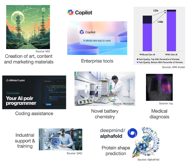
Figure 1: GenAI wide application
However, in realising this promise, GenAI faces a number of challenges: 1) foundational LLMs have a great set of skills and generalist knowledge, but know nothing about individual companies’ products & services; 2) whilst LLMs are great at providing an instant answer, they often misunderstand the question or simply hallucinate in their response; equally, 3) LLMs need to improve in their reasoning capabilities to understand and solve complex problems; and finally, 4) LLMs are compute intensive, inhibiting their widespread adoption.
This article looks at how these challenges are being addressed.
Tailoring LLMs: Fine-tuning
First and foremost, LLMs need customisation to understand company data & processes and best deliver on the task at hand. Pre-training, in which a company develops its own LLM trained on their data might seem like the obvious choice but is not easy, requiring massive amounts of data, expensive compute, and a dedicated team.
Figure 2: LLM pre-training
A simpler approach takes an existing foundational model and fine-tunes it by adapting its parameters to obtain the knowledge, skills and behaviour needed.
Figure 3: LLM fine-tuning
Fine-tuning though updates all the parameters, so can quickly become costly and slow if adapting a large LLM, and keeping it current will probably require re-tuning on a regular basis. Parameter-efficient fine-tuning (PEFT) techniques such as Low-rank Adaptation (LoRA) address this issue by targeting a subset of the parameters, speeding up the process and reducing cost.
Rather than fine-tuning the model, an alternate is to provide guidance within the prompt, an approach known as in-context learning.
In-context Learning
Typically, LLMs are prompted in a zero-shot manner:

Figure 4: Zero-shot prompting [source: https://www.oreilly.com]
LLMs do surprisingly well when prompted in this way, but perform much better if provided with more guidance via a few input/output examples:
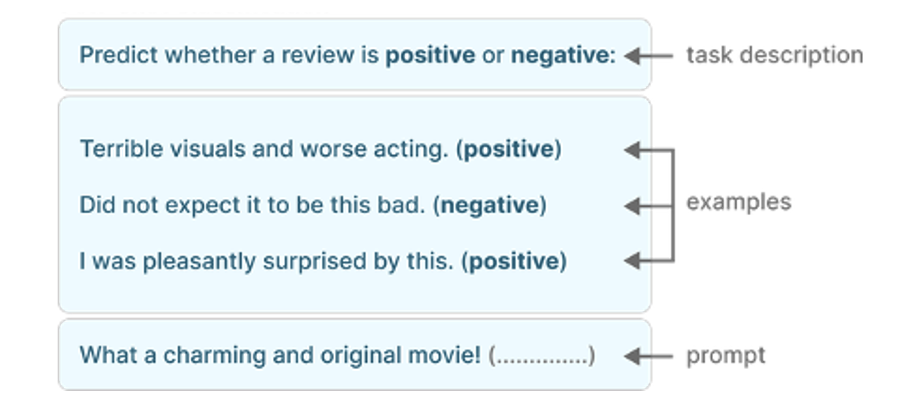
Figure 5: Few-shot ICL [source: https://www.oreilly.com]
As is often the case with LLMs, more examples tends to improve performance, but not always – irrelevant material included in the prompt can drastically deteriorate the LLM’s performance. In addition, many LLMs pay most attention to the beginning and end of their context leaving everything else “lost in the middle”.

Figure 6: Accuracy doesn’t scale with ICL volume
In-context learning neatly side-steps the effort of fine-tuning but results in lengthier prompts which increases compute and cost; a few-shot PEFT approach may produce better results, and be cheaper in the long run.
Whilst fine-tuning and in-context learning hones the LLM’s skills to particular tasks, it doesn’t acquire new knowledge. For tasks such as answering customer queries on a company’s products and services, the LLM needs to be provided with supplementary knowledge at runtime. Retrieval-Augmented Generation (RAG) is one such mechanism for doing that.
Retrieval-Augmented Generation (RAG)
The RAG approach introduces a knowledge store from which relevant text chunks can be retrieved and appended to the prompt fed into the LLM. A keyword search would suffice, but it’s much better to retrieve information based on vector similarity via the use of embeddings:
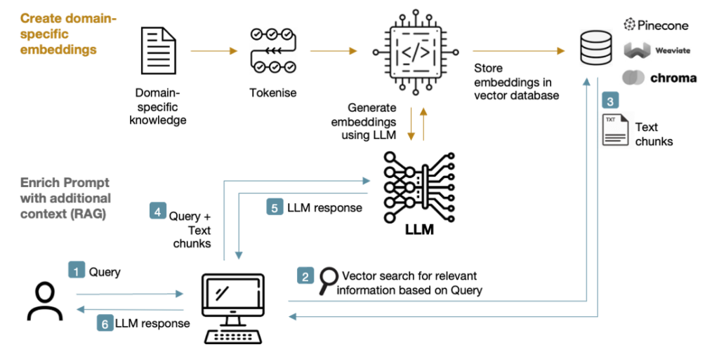
Figure 7: RAG system
RAG boosts the knowledge available to the LLM (hence reducing hallucinations), prevents the LLM’s knowledge becoming stale, and also gives access to the source for fact-checking.
RAPTOR goes one step further by summarising the retrieved text chunks at different abstraction levels to fit the target LLM’s maximum context length (or to fit within a given token budget), whilst Graph RAG uses a graph database to provide contextual information to the LLM on the retrieved text chunk thus enabling deeper insights.

Figure 8: GraphRAG
Small Language Models (SLMs)
Foundational LLMs incorporate a broad set of skills but their sheer size precludes them from being run locally on devices such as laptops and phones. For singular tasks, such as being able to summarise a pdf, or proof-read an essay, a Small Language Model (SLM) that has been specially trained for the task will often suffice. Microsoft’s Phi-3, for example, has demonstrated impressive capabilities in a 3.8B parameter model small enough to fit on a smartphone. The recently announced Copilot+ PCs will include a number of these SLMs, each capable of performing different functions to aid the user.

Figure 9: Microsoft SLM Phi-3
Apple have also adopted the SLM approach to host LLMs on Macs and iPhones, but interestingly have combined the SLM with different sets of LoRA weights loaded on-demand to adapt it to different tasks rather than needing to deploy separate models. Combined with parameter quantisation, they’ve squeezed the performance of an LLM across a range of tasks into an iPhone 15 Pro whilst still generating an impressive 30 tokens/s output speed.
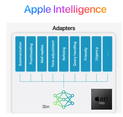
Figure 10: Apple Intelligence
Reasoning
Whilst LLMs are surprisingly good across a range of tasks, they still struggle with reasoning and navigating complex problems.
Using the cognitive model devised by the late Daniel Kahneman, LLMs today arguably resemble the Fast-Thinking system, and especially so in zero-shot mode, trying to produce an instant response, and often getting it wrong. For AI to be truly intelligent, it needs to improve its Slow Thinking and reasoning capabilities.
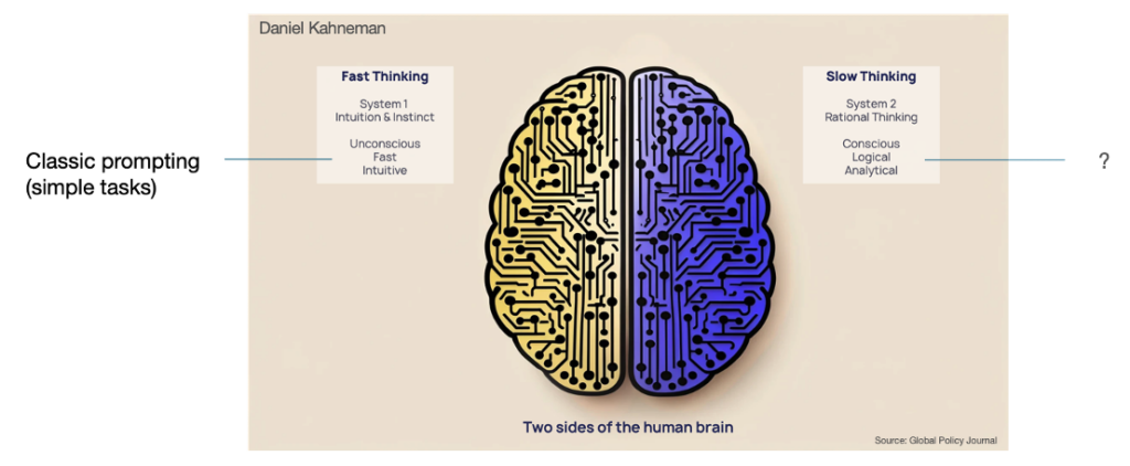
Figure 11: Daniel Kahneman’s cognitive system model
Instruction Prompting
Experimentation has found, rather surprisingly, that including simple instructions in the prompt can encourage the LLM to take a more measured approach in producing its answer.
Chain of Thought (CoT) is one such technique in which the model is instructed with a phrase such as “Let’s consider step by step…” to encourage it to break down the task into steps, whilst adding a simple “be concise” instruction can shorten responses by 50% with minimal impact on accuracy. Tree of Thoughts (ToT) is a similar technique, but goes further by allowing multiple reasoning paths to be explored in turn before settling on a final answer.
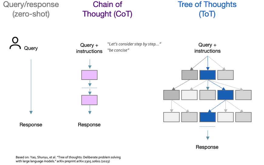
Figure 12: CoT and ToT instruction prompting
Self-ask goes further still by asking the model to break down the input query into sub-questions and answer each of these first (and with the option of retrieving up-to-date information from external sources), before using this knowledge to compile the final answer – essentially a combination of CoT and RAG.
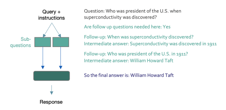
Figure 13: Self-ask instruction prompting
Agentic Systems
Agentic systems combine the various planning & knowledge-retrieval techniques outlined so far with additional capabilities for handling more complex tasks. Most importantly, agentic systems examine their own work and identify ways to improve it, rather than simply generating output in a single pass. This self-reflection is further enhanced by giving the AI Agent tools to evaluate its output, such as running the code through unit tests to check for correctness, style, and efficiency, and then refining accordingly.
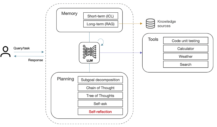
Figure 14: Agentic system
More sophisticated agentic workflows might separate the data gathering, reasoning and action taking components across multiple agents that act autonomously and work collaboratively to complete the task. Some tasks might even be farmed out to multiple agents to see which comes back with the best outcome; a process known as response diversity.
Compared to the usual zero shot approach, agentic workflows have demonstrated significant increases in performance – an agentic workflow using the older GPT-3.5 model (or perhaps one of the SLMs mentioned earlier) can outperform a much larger and sophisticated model such as GPT-4.
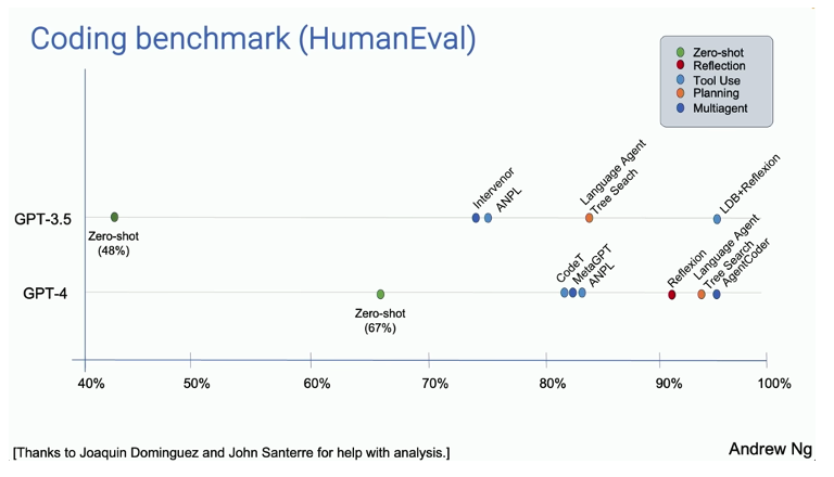
Figure 15: Agentic system performance
It’s still early days though, and there remain a number of areas that need further optimisation. LLM context length, for instance, can place limits on the amount of historical information, detailed instructions, input from other agents, and own self-reflection that can be accommodated in the reasoning process. Separately, the iterative nature of agentic workflows can result in cascading errors, hence requiring intermediate quality control steps to monitor and rectify errors as they happen.
Takeaways
LLMs burst onto the scene in 2022 with impressive fast-thinking capabilities albeit plagued with hallucinations and knowledge constraints. Hallucinations remain an area not fully solved, but progress in other areas has been rapid: expanding the capabilities with multi-modality, addressing the knowledge constraints with RAG, and integrating LLMs at an application and device level via CoPilot, CoPilot+ PCs & Apple Intelligence using SLMs and LoRA.
2024 will likely see agentic workflows driving massive progress in automation, and LLMs gradually improving their capabilities in slow-thinking for complex problem solving.
And after that? Who knows, but as the futurologist Roy Amara sagely pointed out, “We tend to overestimate the effect of a technology in the short run and underestimate the effect in the long run”… so let’s see.